MIS semiconductor device and method of fabricating the same

a semiconductor device and semiconductor technology, applied in the direction of semiconductor devices, basic electric elements, electrical appliances, etc., can solve the problems of increasing the length of wiring, the inability to achieve, and thus to a greater variance of transistor characteristics, so as to suppress the short-channel effect and reduce the variance of channel length

Inactive Publication Date: 2005-04-14
KK TOSHIBA
View PDF12 Cites 37 Cited by
  • Summary
  • Abstract
  • Description
  • Claims
  • Application Information

AI Technical Summary

Benefits of technology

[0033] The present invention has been made in consideration of the above problems, and its object is to provide a semiconductor device and a m

Problems solved by technology

Because of this, a variance occurs among gate electrodes and it leads to a variance in channel length and thus to a greater variance in transistor characteristics.
On the other hand, with miniaturization of semiconductor ICs, fine transistors and wiring are arranged very dense and the length of wiring increases.
Even if the operation speed of transistors is to be increased based on the miniaturization, this cannot be achieved due to a parasitic capacitance and resistance between transistors and wiring.
This contradicts the pur

Method used


Image

  • MIS semiconductor device and method of fabricating the same
  • MIS semiconductor device and method of fabricating the same
  • MIS semiconductor device and method of fabricating the same

Examples


first embodiment

[0158] (First Embodiment)

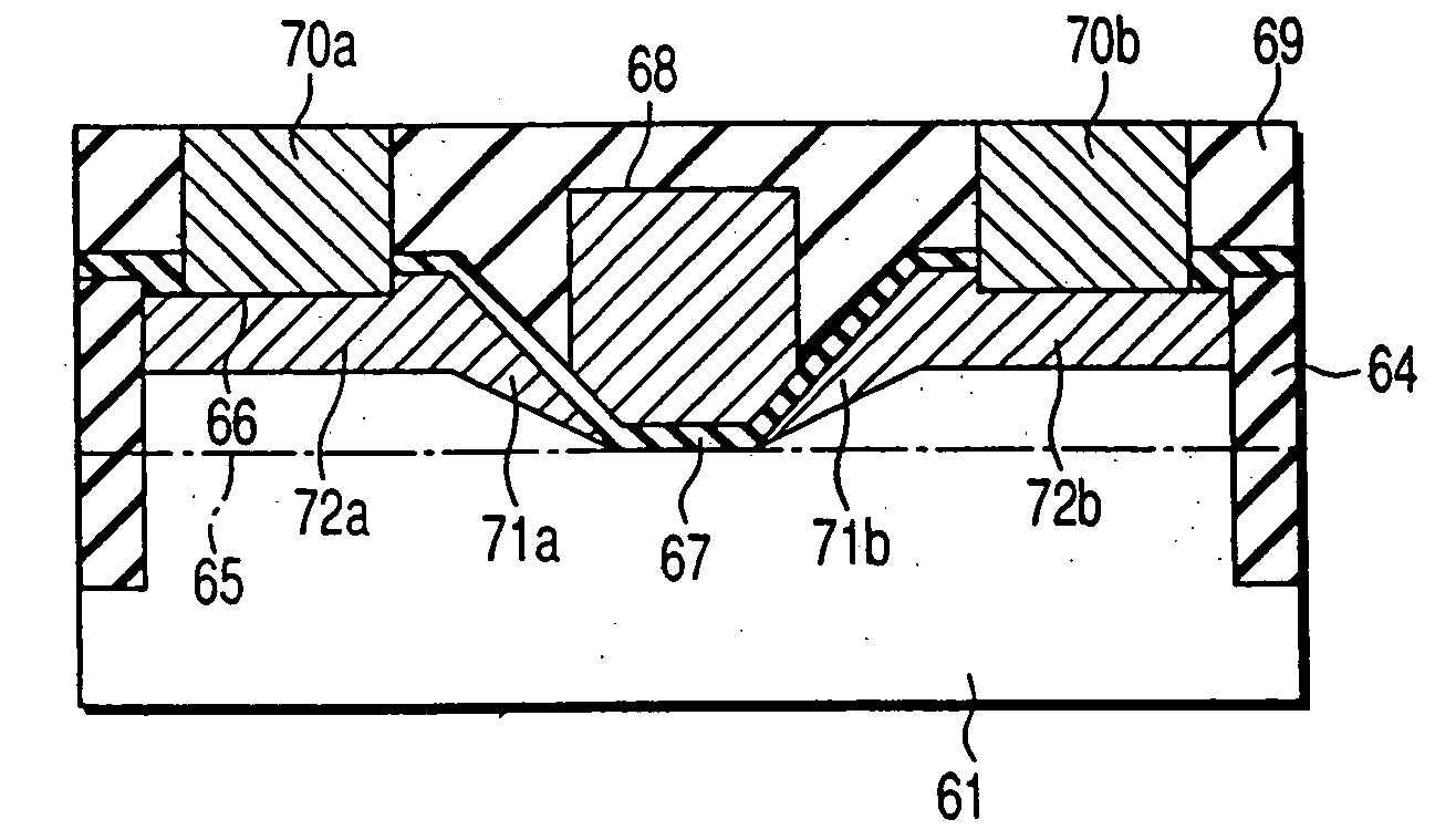
[0159]FIGS. 6A to 9 are views for describing a semiconductor device (concave-type MIS transistor) according to a first embodiment of the invention. FIGS. 6A to 6D and FIG. 9 are views for describing the structure of the semiconductor device according to this embodiment, and FIGS. 7A to 7D and FIGS. 8A to 8D are cross-sectional views showing manufacturing steps of the semiconductor device. FIG. 6A is a plan view of the semiconductor device. FIG. 6B is a cross-sectional view taken along line 6A-6A′ in FIG. 6A. FIG. 6C is a cross-sectional view taken along line 6B-6B′ in FIG. 6A, and FIG. 6D is a cross-sectional view taken along line 6C-6C′ in FIG. 6A. This embodiment is directed to an n-channel MIS transistor. If the conductivity types of respective structural portions are reversed, the following description will apply to a p-channel MIS transistor.

[0160] In FIG. 6B, numeral 61 denotes a p-type silicon substrate using a (100) plane, and its impurity concentra...

second embodiment

[0186] (Second Embodiment)

[0187]FIGS. 10A to 10E are cross-sectional views illustrating steps of manufacturing a transistor structure according to a second embodiment of the invention, wherein the transistor structure has a channel bottom surface with a radius of curvature. In this embodiment the distance between the gate electrode and the contact portion on the mask plane is zero and the contact portion is formed on the inclined source / drain in a self-alignment manner with respect to the gate electrode.

[0188] A description will now be given of a method of manufacturing a concave-type MIS transistor according to the present embodiment.

[0189] A SiO2 film 91 which is 0.02 μm thick is formed on a silicon substrate 61 in an active region. An Si3N4 film 101 which is 0.5 μm thick is then deposited. Using a desired photoresist pattern (not shown) as a mask, an opening is formed in the Si3N4 film 101. Subsequently, as shown in FIG. 10A, using the Si3N4 film 101 as a mask, the silicon subs...

third embodiment

[0203] (Third Embodiment)

[0204]FIG. 11 is a cross-sectional view showing the whole structure of a semiconductor device according to a third embodiment of the present invention. The semiconductor device of this embodiment is a modification of the first embodiment, wherein impurity regions 121a and 121b are added to the first source diffusion layer 71a and first drain diffusion layer 71b by controlling the conditions for the ion implantation 101 shown in FIG. 8B (first embodiment) or the subsequent activation anneal.

[0205] As is shown in FIG. 11, corner portions of the channel plane 65 are covered by the first source diffusion layer 71a and first drain diffusion layer 71b, and thus the impurity regions 121a and 121b covering the corner portions are formed. In this structure, the carrier density of the corner portions of the channel plane 65, which are continuous with the accumulation layers formed in the first source diffusion layer 71a and first drain diffusion layer 71b at the end ...


PUM


Abstract

A MIS type semiconductor device comprises a semiconductor layer provided with a recess portion having a side wall with an obtuse angle at least at a portion of the recess portion, a gate electrode formed over a bottom surface of the recess portion, with a gate insulating film interposed, a source region and a drain region formed on sides of the gate electrode with an insulating film interposed, such that boundary planes between the source region and the drain region, on one hand, and the insulating film, on the other hand, are formed in the semiconductor layer at an angle to a surface of the semiconductor layer, and wiring portions for contact with the surface of the semiconductor layer. Wherein an edge of the gate electrode is located inside the recess portion provided in the semiconductor layer, and there is provided at least one of a mutually opposed portion between the gate electrode and the source region and a mutually opposed portion between the gate electrode and the drain region, whereby at least one of a portion of the source region and a portion of the drain region, which lie in the associated mutually opposed portions, functions as an accumulation layer.

Description

BACKGROUND OF THE INVENTION [0001] The present invention relates generally to a MIS semiconductor device and a method of fabricating the same, and more particularly to improvements of a source region and a drain region. [0002] In order to meet a demand for a higher performance based on a higher integration density achieved by modern finer processing, when semiconductor integrated circuits (ICs) are fabricated, a gate electrode of a transistor is processed with a highest possible level of lithographic processing. Because of this, a variance occurs among gate electrodes and it leads to a variance in channel length and thus to a greater variance in transistor characteristics. Consequently, the product yield decreases. On the other hand, with miniaturization of semiconductor ICs, fine transistors and wiring are arranged very dense and the length of wiring increases. Even if the operation speed of transistors is to be increased based on the miniaturization, this cannot be achieved due to...

Claims


Application Information

Patent Timeline
IPC IPC(8): H01L21/336H01L29/78
CPCH01L29/66545H01L29/7834H01L29/66628H01L29/66621
Inventor NISHINOHARA, KAZUMI
Owner KK TOSHIBA
Why Eureka
Try Eureka