Leadframe for use in a semiconductor package

Active Publication Date: 2005-04-14
INFINEON TECH AG
View PDF19 Cites 5 Cited by
  • Summary
  • Abstract
  • Description
  • Claims
  • Application Information

AI Technical Summary

Benefits of technology

[0012] A semiconductor chip is then attached to the die mounting area and electrical connections by, for example, bond wires, are made between the semiconductor chip and the inner end of the lead fingers. The die, bond wires and inner portion of the lead fingers are encapsulated. The external leads are plated with solder and then the individual packages are split from the leadframe strip. The external leads which are plated with solder enable the package to be easily soldered to an external circuit, such as a printed circuit board.
[0013] In accordance with a further embodiment of the present invention method, the metal deposit comprises Zn, Pb, Sn, Ni, Fe or Cr and the leadframe comprises Cu or a Cu-alloy. The metal can be deposited by electroplating although any depositing method can be employed. Electroplating is desirable in that it is cost-effective, fast, plating baths are readily available, masking processes are known and it is easily incorporated in the existing manufacturing process.
[0014] The leadframe is masked so as to deposit the metal on the desired areas. The metal deposit is positioned so as to prevent corrosion of the leadframe in a particular manufacturing process for a particular sem

Problems solved by technology

Copper leadframes of encapsulated semiconductor packages can corrode during the manufacturing and assembly process.
This is undesirable as oxidation and corrosion of the copper surface leads to poor electrical contacts between both the semiconductor chip and the leadframe, as well as, between the leadframe and the external circuit board.
The silver coating takes up approximately 40% of the cost of the frame, thereby

Method used


Image

  • Leadframe for use in a semiconductor package
  • Leadframe for use in a semiconductor package

Examples


Example

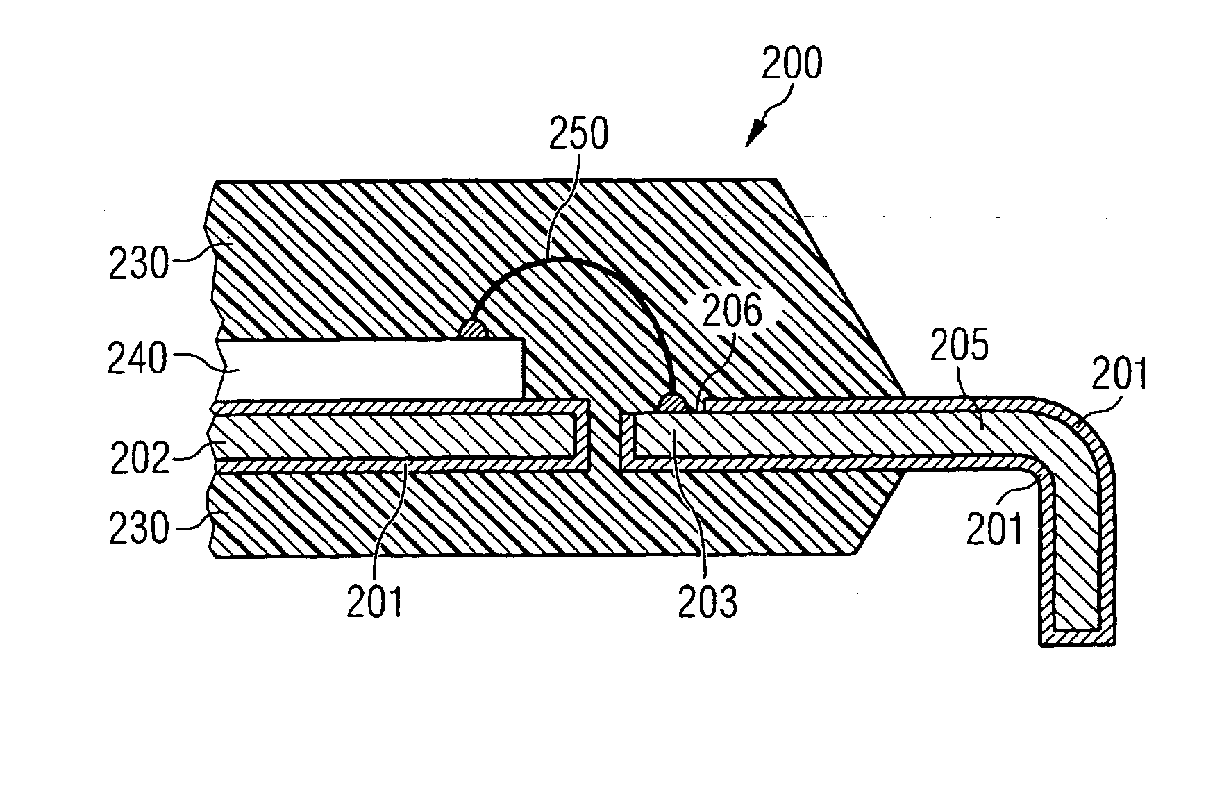
[0021]FIG. 1 shows the top view of a section of a copper leadframe strip including spots of zinc. The section of leadframe may be used to mount a semiconductor chip (not shown) in an encapsulated leadframe package (not shown).

[0022] A rectangular die mounting area 2 is located in the center of a section of leadframe strip 1 and it is surrounded by a plurality of lead fingers 3. There is an inner support rectangle including horizontal support bars 4 and vertical support bars 5 connecting the lead fingers 3 at a point along their length. An outer rectangular support frame 6 connects the outer ends of lead fingers 3. The die mounting area 2 is connected by two horizontal support bars 7 to support vertical support bars 5.

[0023] The support bars 4, 5, 6 and 7 are removed at the end of the manufacturing process to create a free-standing die mounting area 2 and separate lead fingers 3.

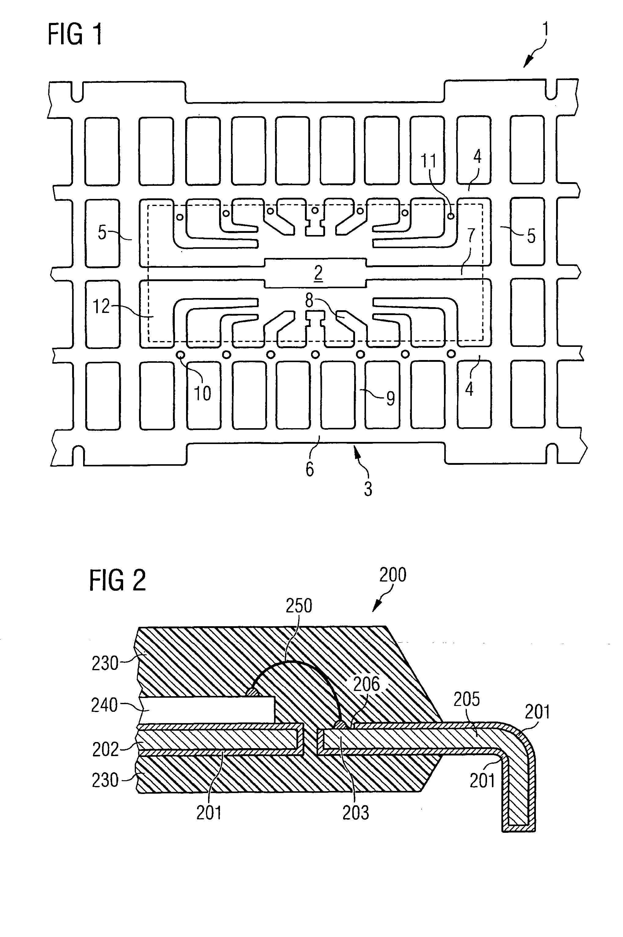
[0024] The central area of the leadframe including the die mounting area 2 and inner portion of lead fi...


PUM


Abstract

A leadframe comprises a die mounting area, a plurality of lead fingers and a metal deposit having a negative electrochemical potential with respect to a standard H2 half cell. A semiconductor package comprises the leadframe and a semiconductor chip having a plurality of contact areas mounted to the die mounting area and electrically connected to the inner ends of the lead fingers of the leadframe by a plurality of bond wires. The semiconductor chip, the bond wires and inner portions of the lead fingers are encapsulated by a plastic housing.

Description

CROSS REFERENCE TO RELATED APPLICATIONS [0001] This application claims priority under 35 U.S.C. §119 to European Application No. EP 03023224.3, filed on Oct. 13, 2003, and entitled “LEADFRAME,” the disclosure of which is incorporated herein by reference in its entirety. FIELD OF THE INVENTION [0002] The present invention relates to a leadframe for use in a semi-conductor package. BACKGROUND [0003] Copper leadframes of encapsulated semiconductor packages can corrode during the manufacturing and assembly process. This is undesirable as oxidation and corrosion of the copper surface leads to poor electrical contacts between both the semiconductor chip and the leadframe, as well as, between the leadframe and the external circuit board. [0004] One method of improving the reliability of semiconductor packages is to coat the copper leadframe with a thick silver coating. The silver coating takes up approximately 40% of the cost of the frame, thereby limiting potential future price reductions...

Claims


Application Information

Patent Timeline
IPC IPC(8): H01L23/495
CPCH01L23/49582H01L2224/48091H01L2224/48247H01L2924/01046H01L2924/00014H01L2924/01078H01L2924/15747H01L24/48H01L2224/45099H01L2924/00H01L24/97H01L2224/97H01L2924/181H01L2224/85H01L2924/00012
Inventor GOH, KOH HOOKEONG, BUN-HIN
Owner INFINEON TECH AG
Why Eureka
Try Eureka