Surface acoustic wave element and electronic equipment provided with the element

a technology of surface acoustic wave and electronic equipment, which is applied in the direction of impedence networks, electrical equipment, etc., can solve the problems of insufficient improvement of loss of matching frequency of surface acoustic waves of idt and surface acoustic waves of reflectors, and impaired impedance characteristics and insertion losses. , to achieve the effect of improving the impedance characteristic and insertion loss

Inactive Publication Date: 2005-04-14
SEIKO EPSON CORP
View PDF8 Cites 25 Cited by
  • Summary
  • Abstract
  • Description
  • Claims
  • Application Information

AI Technical Summary

Benefits of technology

[0016] The present invention has been made in view of the problem in the prior art described above, and therefore it is an object of the present invention to provide a surface acoustic wave element employing a subs

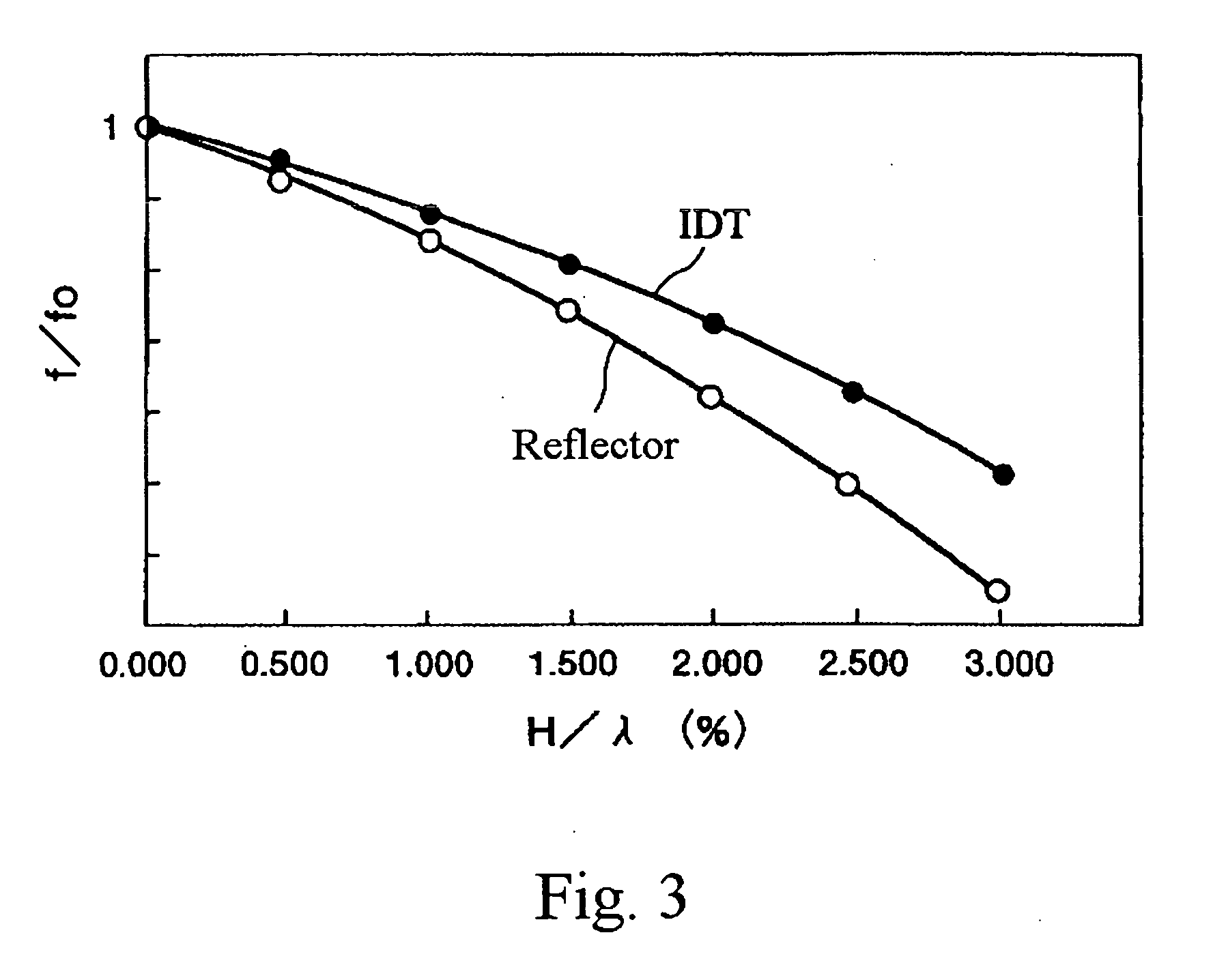
Problems solved by technology

However, when the thickness of the IDT and the reflector is made large, matching of the frequency of the surface acoustic wave of the IDT and the frequency of the surface acoustic wave of the reflector tends to be lost.
As a result, a phenomenon in which the impedance characteristic and the insertion loss are likely to be

Method used


Image

  • Surface acoustic wave element and electronic equipment provided with the element
  • Surface acoustic wave element and electronic equipment provided with the element
  • Surface acoustic wave element and electronic equipment provided with the element

Examples


example 1

(Example 1)

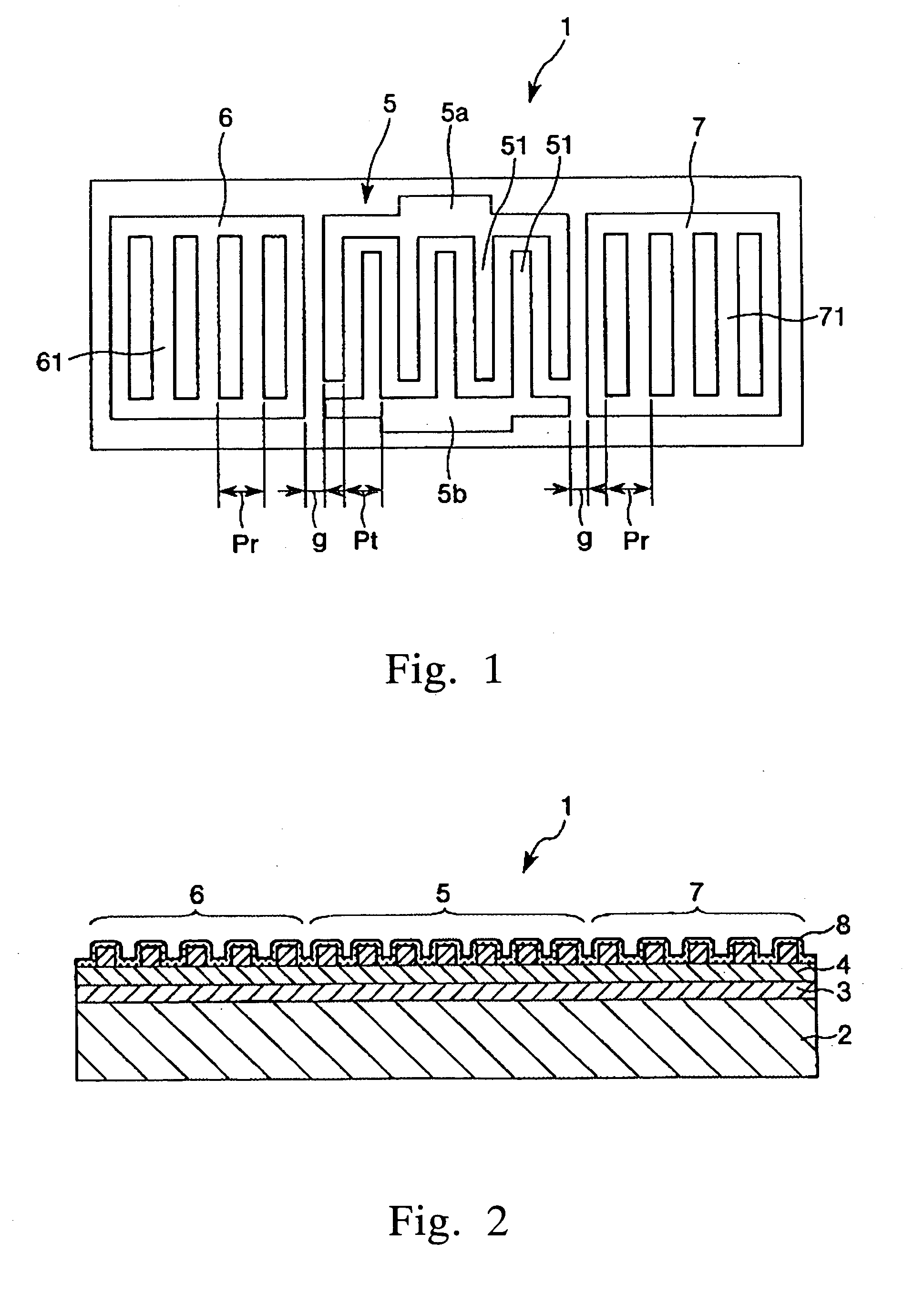
[0116] First, a silicon substrate having the average thickness of 0.4 mm was prepared as the substrate.

[0117] Then, a diamond layer (intermediate layer) having the average thickness of 10 μm and a zinc oxide layer (piezoelectric layer) having the average thickness of 400 nm were formed on the substrate by laminating them sequentially. Here, the average thickness of the zinc oxide layer was 0.1 time the wavelength of the surface acoustic wave.

[0118] Next, aluminum was adhered to the zinc oxide layer by vacuum deposition to form a conductive material layer having the average thickness of 40 nm.

[0119] Next, a resist film corresponding to the shapes of the IDT and the reflectors were formed on the conductive material layer.

[0120] Next, the IDT and the reflectors were formed by removing unnecessary portions of the conductive material layer by dry etching using the resist film as a mask.

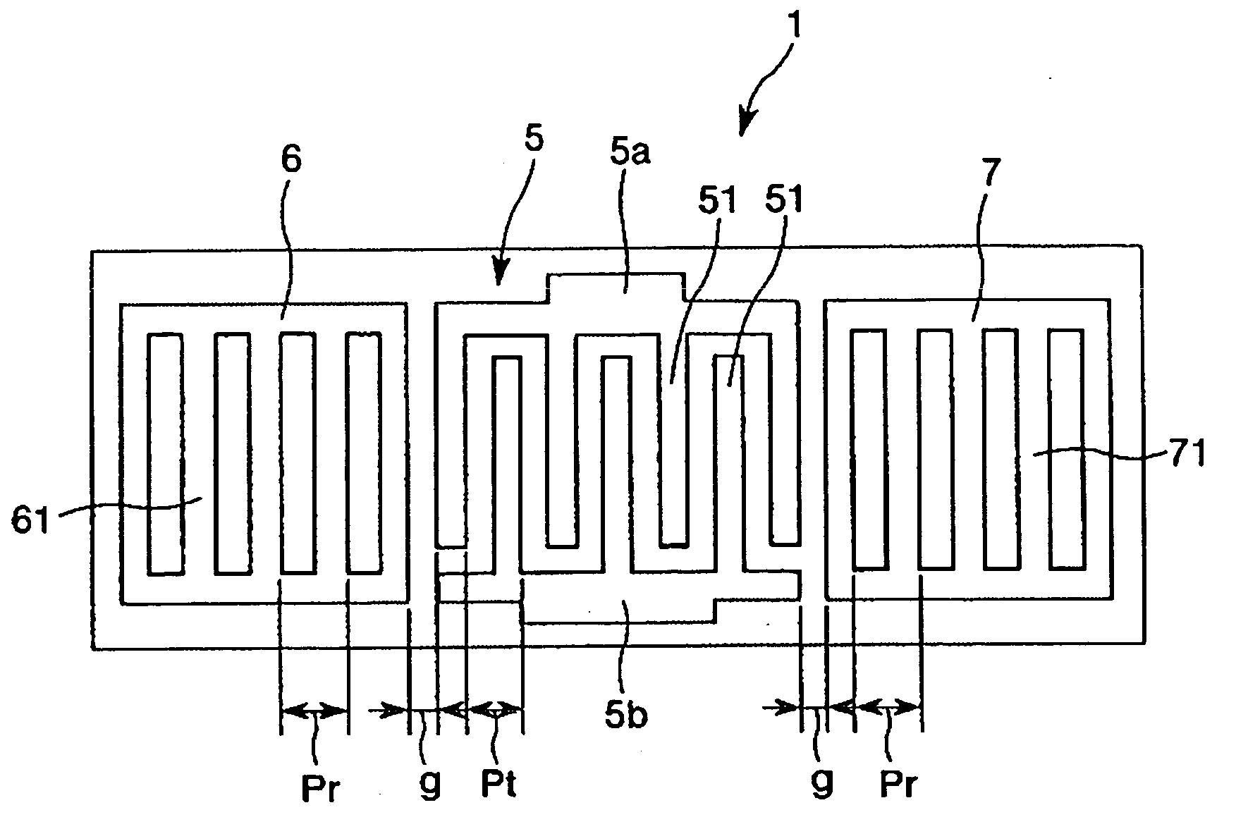
[0121] Here, the wavelength of the surface acoustic wave, the electrode finger pitch Pt...

example 2

(Example 2)

[0123] The surface acoustic wave element as shown in FIG. 5 and FIG. 6 was obtained in a manner similar to the first example except for the formation of the IDT for input and the IDT for output.

[0124] Here, the electrode finger pitch Pt for the IDTs, the reflecting body pitch Pr for the reflectors and the separation distance g between the IDT and the reflector were set respectively to be the same as in the example 1.


PUM


Abstract

A surface acoustic wave element 1 includes a substrate 2, an intermediate layer and a piezoelectric layer 4 laminated on the substrate 2, an IDT 5 disposed on the piezoelectric layer 4, a pair of reflectors 6 and 7 arranged on both sides of the IDT 5, and a protective layer 8 provided so as to cover the IDT 5 and the reflectors 6 and 7. The IDT 5, that is each of the electrode 5a and 5b, has a plurality of electrode fingers 51 juxtaposed with a prescribed spacing and the reflectors 6 and 7 have respectively a plurality of reflecting bodies 61 and 71. Further, the pitch Pr of the reflecting body of each reflector 6 and 7 is set to be smaller than the pitch Pt of the electrode finger of the IDT 5 and the ratio Pr/Pt is preferably set to be in the range of 0.7 to 0.9995. According to the surface acoustic wave element 1, the impedance characteristic and the insertion loss can be improved. Furthermore, electronic equipment having such surface acoustic wave element is provided.

Description

BACKGROUND OF THE INVENTION [0001] 1. Field of the Invention [0002] The present invention relates to a surface acoustic wave element and electronic equipment provided with the element. [0003] 2. Description of the Prior Art [0004] A wave which is propagated by concentrating its energy in the vicinity of the surface of a propagation medium is known as a Surface Acoustic Wave (SAW). [0005] A surface acoustic wave element is a device utilizing such a surface acoustic wave. The surface acoustic wave element is used in a band pass filter for communication equipment such as a mobile telephone, a resonator as a reference clock, a delay element for signal processing (in particular, a fourier transform functional element), various kinds of sensors such as a pressure sensor and a temperature sensor, an optical deflector, and the like. [0006] A surface acoustic wave element used as a filter or a resonator, for example, comprises a piezoelectric base body as the propagation medium of the surfac...

Claims


Application Information

Patent Timeline
IPC IPC(8): H03H9/25H03H9/02H03H9/145
CPCH03H9/02574H03H9/25
Inventor FUNASAKA, TSUKASA
Owner SEIKO EPSON CORP
Why Eureka
Try Eureka