Dual damascene structure and method

a damascene and structure technology, applied in the direction of basic electric elements, electrical equipment, electric discharge tubes, etc., can solve the problems of shortening and device failure, copper cannot be directly etched, and the patterning of the insulating layer in the dual damascene process becomes more and more difficult, so as to improve the control of the dual damascene etching process

a damascene and structure technology, applied in the direction of basic electric elements, electrical equipment, electric discharge tubes, etc., can solve the problems of shortening and device failure, copper cannot be directly etched, and the patterning of the insulating layer in the dual damascene process becomes more and more difficult, so as to improve the control of the dual damascene etching process

US20050079706A1Active Publication Date: 2005-04-14INFINEON TECH AG +1

Image

  • Dual damascene structure and method
  • Dual damascene structure and method
  • Dual damascene structure and method

Examples


Embodiment Construction

[0024] The making and using of the presently preferred embodiments are discussed in detail below. It should be appreciated, however, that the present invention provides many applicable inventive concepts that can be embodied in a wide variety of specific contexts. The specific embodiments discussed are merely illustrative of specific ways to make and use the invention, and do not limit the scope of the invention.

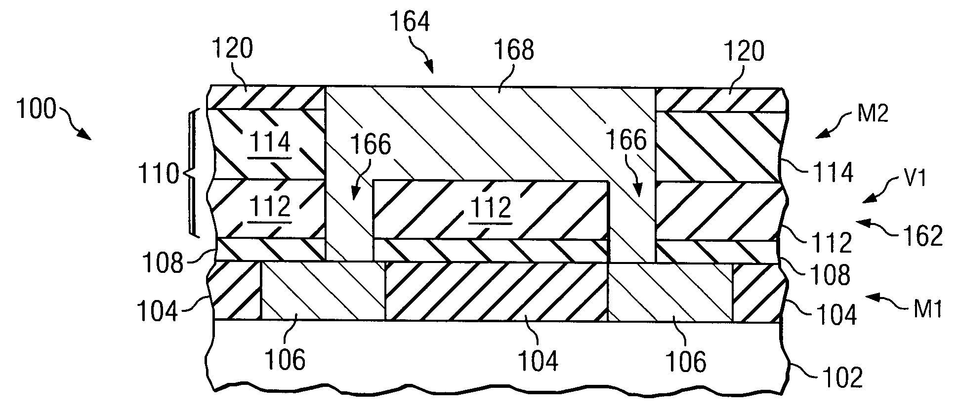
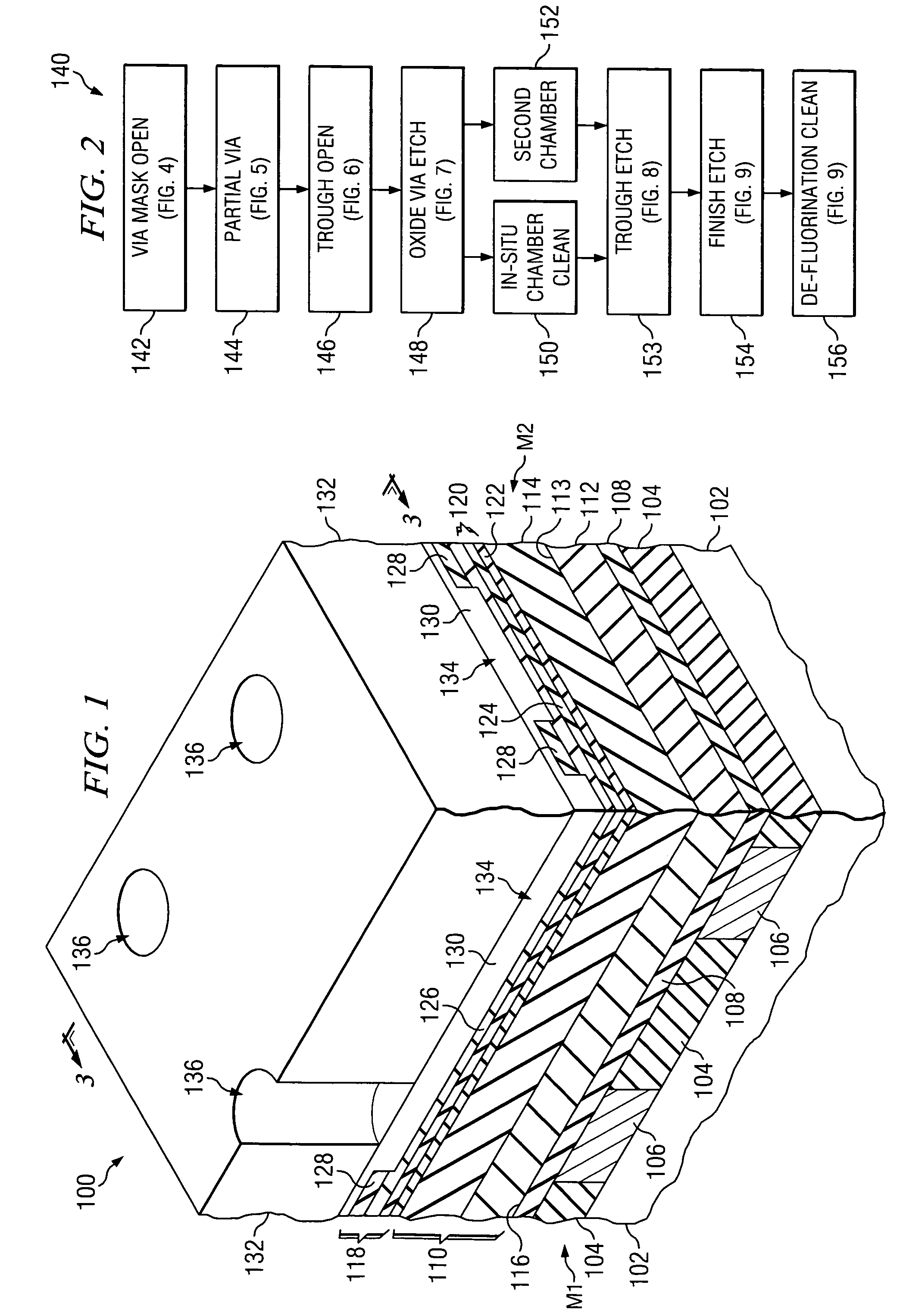
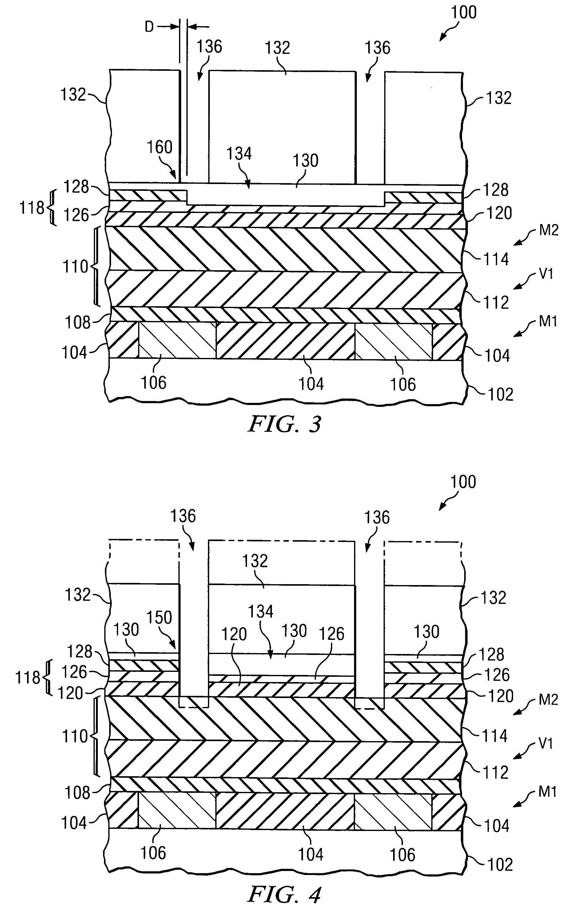
[0025]FIG. 1 shows a perspective view of a dielectric stack 100 in which a dual damascene structure will be fabricated in accordance with an embodiment of the present invention, wherein an insulating layer 110 to be patterned using a dual damascene process comprises a bi-layer of dielectric materials 112 and 114. A first insulating layer 104 which may comprise silicon dioxide or low-dielectric constant materials, for example, is deposited over a workpiece 102. The workpiece may include a semiconductor substrate comprising silicon or other semiconductor materials covered by ...


PUM

PropertyMeasurementUnit
pressureaaaaaaaaaa
dielectric constantaaaaaaaaaa
thicknessaaaaaaaaaa

Abstract

A dual damascene structure and method of fabrication thereof. An insulating layer comprises a first dielectric material and a second dielectric material, the second dielectric material being different from the first dielectric material. First conductive regions having a first pattern are formed in the first dielectric material, and second conductive regions having a second pattern are formed in the second dielectric material, the second pattern being different from the first pattern. One of the first dielectric material and the second dielectric material comprises an organic material, and the other dielectric material comprises an inorganic material. One of the first and second dielectric materials is etchable selective to the other dielectric material. A method of cleaning a semiconductor wafer processing chamber while a wafer remains residing within the chamber is also disclosed.

Description

CROSS-REFERENCE TO RELATED APPLICATIONS [0001] This application relates to the following co-pending and commonly assigned patent applications: Ser. No. ______, filed concurrently herewith, entitled Dual Damascene Structure and Method, which application is hereby incorporated herein by reference.TECHNICAL FIELD [0002] The present invention relates generally to the fabrication of semiconductor devices, and more particularly to the fabrication of a dual damascene structure. BACKGROUND [0003] Semiconductor devices are fabricated by sequentially depositing insulating (or dielectric) layers, conductive layers and semiconductive layers of material over a semiconductor substrate, and patterning the various layers using lithography to form circuit components and elements thereon. A common conductive material used in the past for conductive lines was aluminum, which can be directly etched. For example, a layer of aluminum or aluminum alloy is deposited, a photoresist layer is deposited over t...

Claims


Application Information

Patent Timeline
14 Apr 2005
Publication
US20050079706A1
IPC
H01L21/306; H01L21/311; H01L21/3213; H01L21/4763; H01L21/768
CPC
H01J37/32862; H01L21/02046; H01L21/31116; H01L21/76835; H01L21/31144; H01L21/32136; H01L21/76811; H01L21/31138
Inventors
KUMAR, KAUSHIK; LA TULIPE, DOUGLAS C.