Mobile terminal, circuit board, circuit board design aiding apparatus and method, design aiding program, and storage medium having stored therein design aiding program

a technology of circuit board and design aiding apparatus, applied in the direction of unauthorized memory use protection, instruments, pulse techniques, etc., can solve the problems of large challenge to establish security systems, communications interception, content converted into digital information vulnerable to fraudulent acquisition, etc., and achieve the effect of improving the resistance to manipulation

Inactive Publication Date: 2005-04-14
PANASONIC CORP
View PDF9 Cites 38 Cited by
  • Summary
  • Abstract
  • Description
  • Claims
  • Application Information

AI Technical Summary

Benefits of technology

[0009] Therefore, an object of the present invention is to provide a circuit board in which tamper resistance is improved by making probing by third parties difficult, while solving problems associated with the current techniques and manufacturing costs. In addition, another object of the present invention is to provide a design aiding apparatus and method for such a circuit board, a design aiding program, and a storage medium having stored therein the design aiding program.

Problems solved by technology

The content converted into digital information is vulnerable to fraudulent acquisition by communications interception, wiretapping, spoofing, or the like, and fraudulent activities such as illegal copies and illegal modification of storage media having stored therein the data of the content.
Thus, it is a great challenge to establish security systems for protecting the rights of content copyright holders and the profits of content distributors.
One of the conditions for improving the tamper resistance of a circuit board in which components and the like are installed and connected by wiring, is the difficulty of probing a signal line which transmits digital information.
The harder it is to read a signal on the circuit board, i.e., the harder it is to perform probing, the harder it gets to analyze or copy digital information by external unauthorized access, and the easier it is to perform probing, the easier it gets to extract a signal, and thus it becomes easy to analyze or copy digital information.
However, in the method in which the circuit section where confidential information is processed is formed in a one-chip IC format or covered by a resin or the like, problems arise that off-the-shell ICs cannot be used, all the chips and wiring on the circuit board need to be taken care of, and the like.
Thus, such methods are impractical in terms of the current techniques and manufacturing costs.
In addition, after the circuit section is formed in a one-chip IC format or covered by a resin, not only third parties but also a developer or designer (hereinafter referred to as a “designer or the like”) cannot verify a confidential signal.
Further, to adopt in circuit boards conventional encryption / authentication techniques for communication, a logic for realizing the techniques needs to be incorporated in all LSIs handling digital information, and thus the adoption of such techniques are also impractical in terms of the current techniques and manufacturing costs.
Moreover, the method in which a signal line for confidential information is covered by a component, as in the case of Japanese Laid-Open Patent Publication No. 2002-299842, has a problem that probing can be easily done by removing the component.
As described above, with the conventional techniques, it is very difficult to completely conceal a signal line of the circuit board, through which confidential information flows.

Method used


Image

  • Mobile terminal, circuit board, circuit board design aiding apparatus and method, design aiding program, and storage medium having stored therein design aiding program
  • Mobile terminal, circuit board, circuit board design aiding apparatus and method, design aiding program, and storage medium having stored therein design aiding program
  • Mobile terminal, circuit board, circuit board design aiding apparatus and method, design aiding program, and storage medium having stored therein design aiding program

Examples


first embodiment

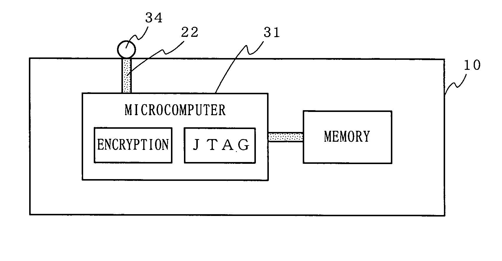
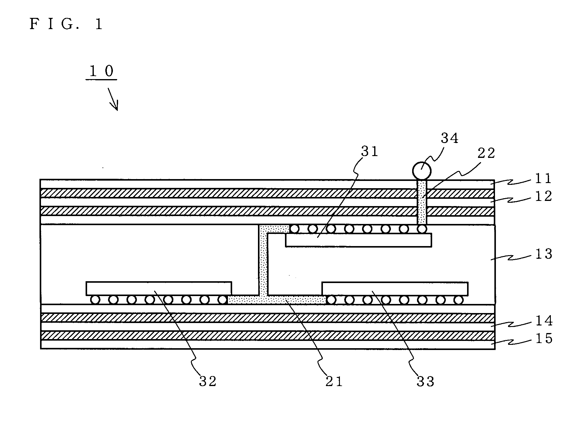
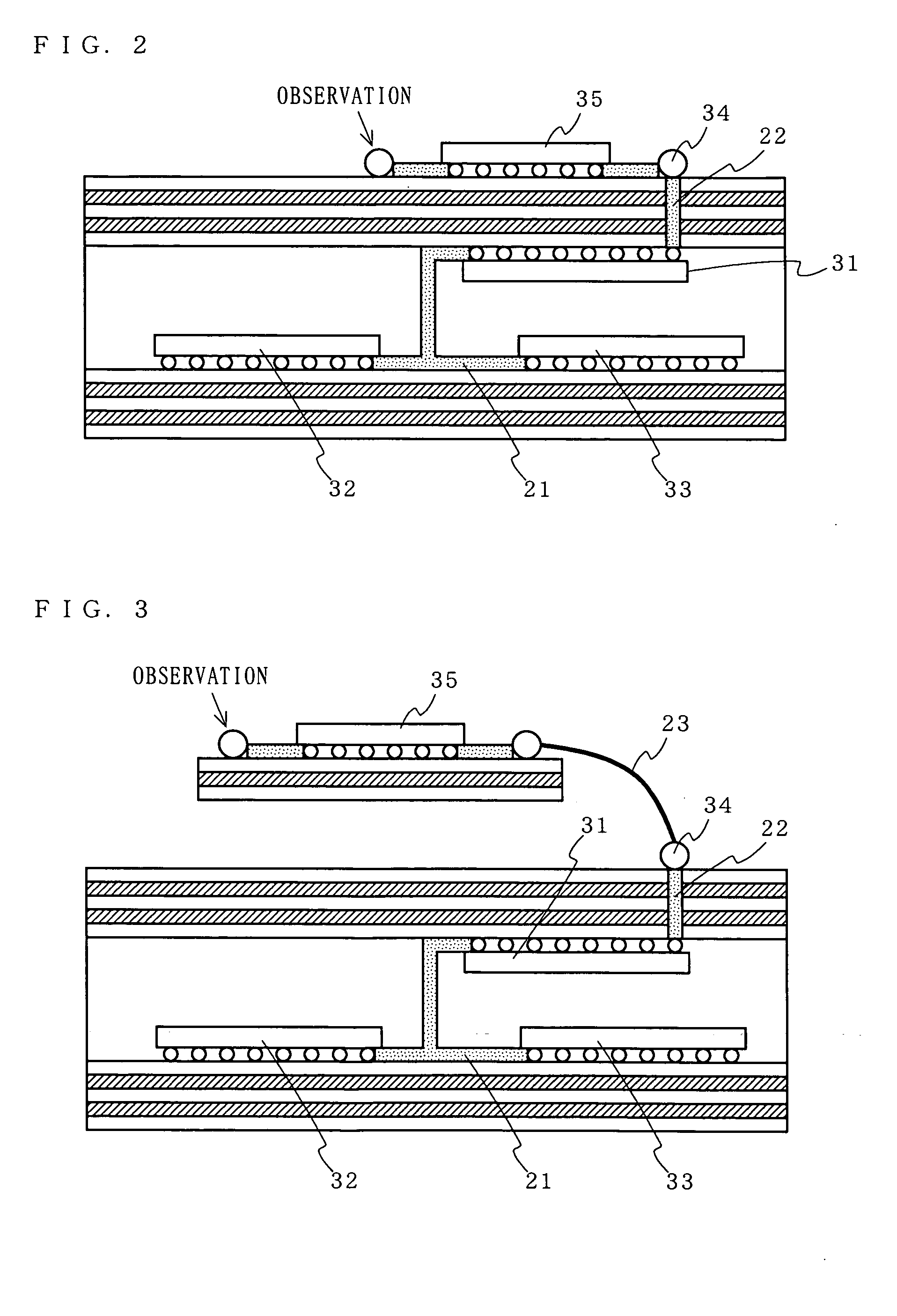
[0033] A circuit board according to a first embodiment of the present invention has a structure in which a signal line for a signal requiring tamper resistance, such as confidential information, is wired in an internal layer and a designer or the like is allowed to observe or control a confidential signal when necessary.

[0034]FIG. 1 is a cross-sectional view of a circuit board 10 having a substrate structure according to the first embodiment of the present invention. As shown in FIG. 1, the circuit board 10 includes an upper substrate 11, an upper multilayer substrate 12, a component-containing layer 13, a lower multilayer substrate 14, and a lower substrate 15. The component-containing layer 13 contains therein components 31, 32, and 33. In FIG. 1, a signal line 21 which interconnects between the components 31, 32, and 33 serves as a signal line through which a signal requiring tamper resistance flows. The signal requiring tamper resistance includes, for example, a signal that a c...

second embodiment

[0049] A circuit board according to a second embodiment of the present invention has a structure in which a signal line for a confidential signal is wired in an internal layer and components whose terminals are exposed, such as a two-terminal component and a QFP (Quad Flat Package) component, are arranged in the internal layer.

[0050]FIG. 6 is a cross-sectional view of a circuit board 40 having a substrate structure according to the second embodiment of the present invention. As shown in FIG. 6, the circuit board 40 includes an upper substrate 41, an upper multilayer substrate 42, a component-containing layer 43, a lower multilayer substrate 44, and a lower substrate 45. A component 61 is placed on the upper substrate 41. The component-containing layer 43 contains therein components 62 and 63. In FIG. 6, a signal line 51 for connecting between the components 62 and 63 serves as a signal line through which a confidential signal requiring tamper resistance flows. The signal line 51 is...

third embodiment

[0053] A third embodiment of the present invention will describe an example where the substrate structures described in the foregoing first and second embodiments are used in mobile terminals such as mobile phones and PDAs.

[0054] As is commonly known, a mobile phone has personal information about the user himself / herself and other people, a password, and the like stored therein. These personal information and password are confidential information that the user does not want third parties to see, and thus preferably have tamper resistance to fraudulent activities. In view of this, a mobile phone may use a circuit board in which a memory component where confidential information is stored and a signal line through which a signal regarding the confidential information flows are all contained in an internal layer of the circuit board. FIGS. 7A and 7B are diagrams showing a specific example of the above-described configuration. Specifically, a non-volatile memory 73 (flash memory) where ...


PUM


Abstract

A circuit board is provided in which tamper resistance is improved by making probing by third parties difficult, while solving problems associated with the current techniques and manufacturing costs. A signal line through which a confidential signal requiring tamper resistance flows and components 32 and 33 connected to the signal line 21 by the terminals thereof, are laid out in a component-containing layer 13 of a circuit board 10. Only a confidential signal having been encrypted through a predetermined component 31 is outputted to an observation point 34 provided on a surface of the circuit board 10. External observation and control of the confidential signal is performed by decoding a cipher provided by the component 31 to the signal which appears at the observation point 34.

Description

BACKGROUND OF THE INVENTION [0001] 1. Field of the Invention [0002] The present invention relates to a mobile terminal, a circuit board, a circuit board design aiding apparatus and method, a design aiding program, and a storage medium having stored therein the design aiding program. More particularly, the present invention relates to a tamper-resistant circuit board, an apparatus and method for aiding the design of the circuit board, a program for performing the method, a computer-readable storage medium having stored therein the program, and a mobile terminal containing the circuit board. [0003] 2. Description of the Background Art [0004] In recent years, with the development of digital information technologies and the explosive popularization of digital information communication infrastructure, it has become more common to process content such as music, images, video, and games, as digital information. The content converted into digital information is vulnerable to fraudulent acqu...

Claims


Application Information

Patent Timeline
Patent Type & Authority Applications(United States)
IPC IPC(8): G06F17/50G06F21/87H05K1/02H05K1/18H05K3/00
CPCG06F17/5068G06F21/87H05K2201/10151H05K1/186H05K3/0005H05K1/0275H01L2224/16225G06F30/39
Inventor NAKAYAMA, TAKESHISAITO, YOSHIYUKIASAHI, TOSHIYUKI
Owner PANASONIC CORP
Why Eureka
Try Eureka