Method and apparatus for producing optical disk substrates

Inactive Publication Date: 2005-04-21
ENERGY CONVERSION DEVICES INC
View PDF4 Cites 16 Cited by
  • Summary
  • Abstract
  • Description
  • Claims
  • Application Information

AI Technical Summary

Benefits of technology

[0020] Another embodiment of the present invention provides a process for hot embossing a thin film (thickness of 0.6 mm or less, preferably 0.25 mm or less) that simultaneously embosses information and track structure on both sides of a polymeric material and accurately punches a centered hole that does not interfere with the reading of the disc.
[0021] Another embodiment of the present invention provides a hot embossing process that stabilizes a web of polymeric material during the hot embossing process to result in a higher quality replication.
[0022] Another embodiment of the present invention provides a hot embossing process that limits and preferably e

Problems solved by technology

Besides lower than desired production rates, injection molding requires complex closed-loop control over numerous parameters.
This makes the overall system a highly complex process, at a point in the process where it may not be desirable.
Furthermore, because the disk manufacturer may not enjoy the same economies of scale that a plastic web manufacturer does, the cost per unit for disks formed with in-line processes may be higher than that for off-line processes.
For example, the present inventors have found that unavoidable variation in web surface texture and web thickness exist and can interfere with fine microstructure reproduction.
These variations result in locally, non-uniform contact pressure between the web and stamper.
In a proces

Method used


Image

  • Method and apparatus for producing optical disk substrates
  • Method and apparatus for producing optical disk substrates
  • Method and apparatus for producing optical disk substrates

Examples


Embodiment Construction

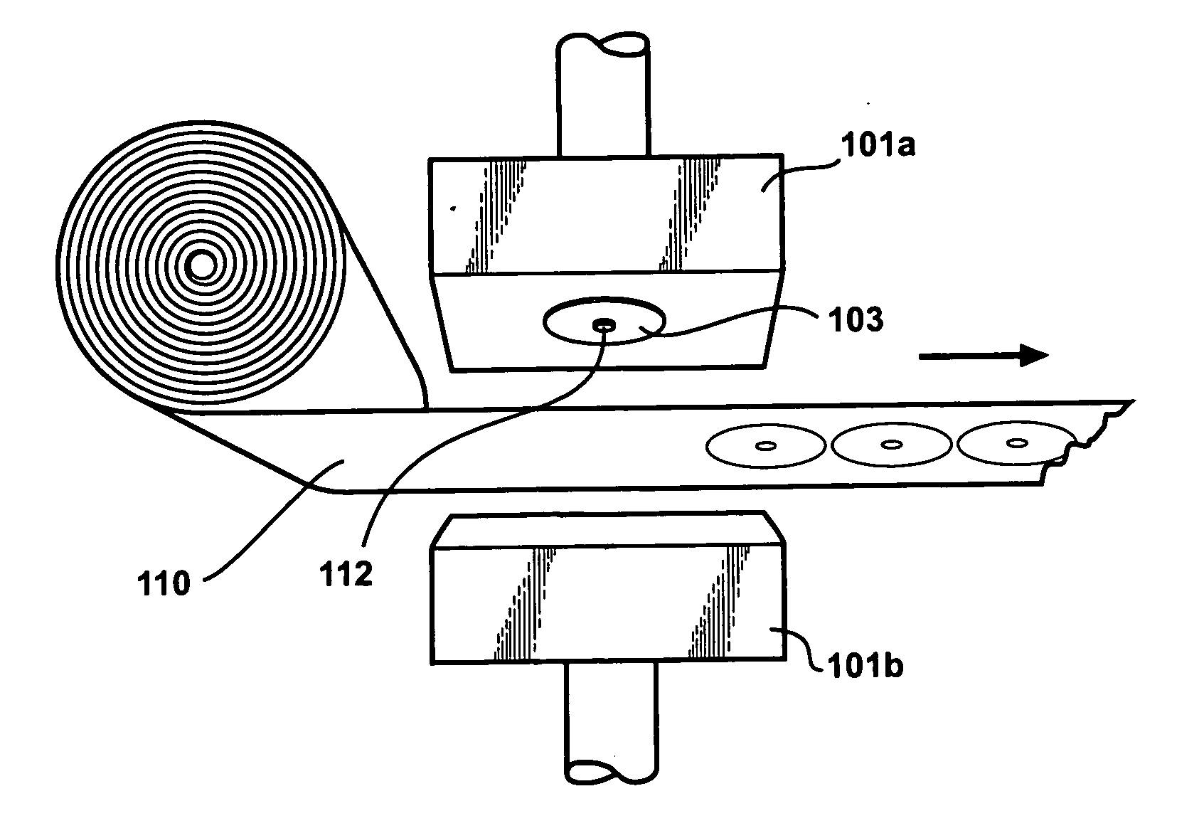
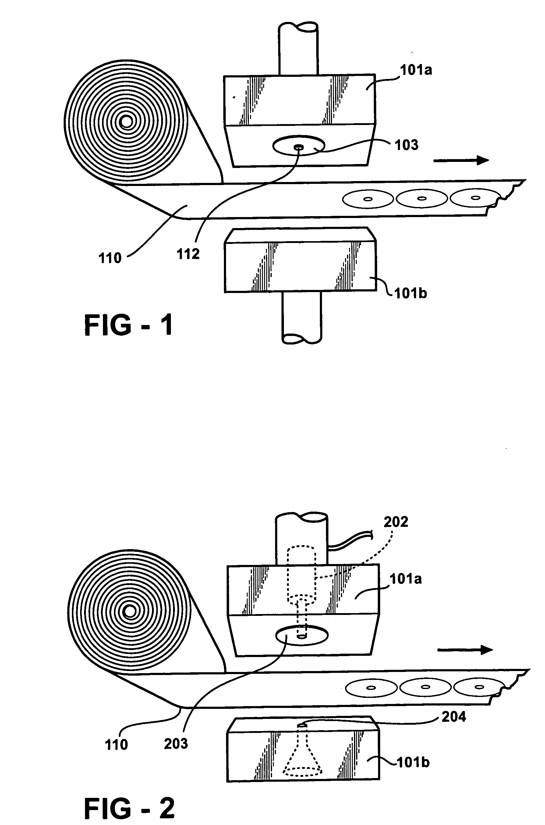
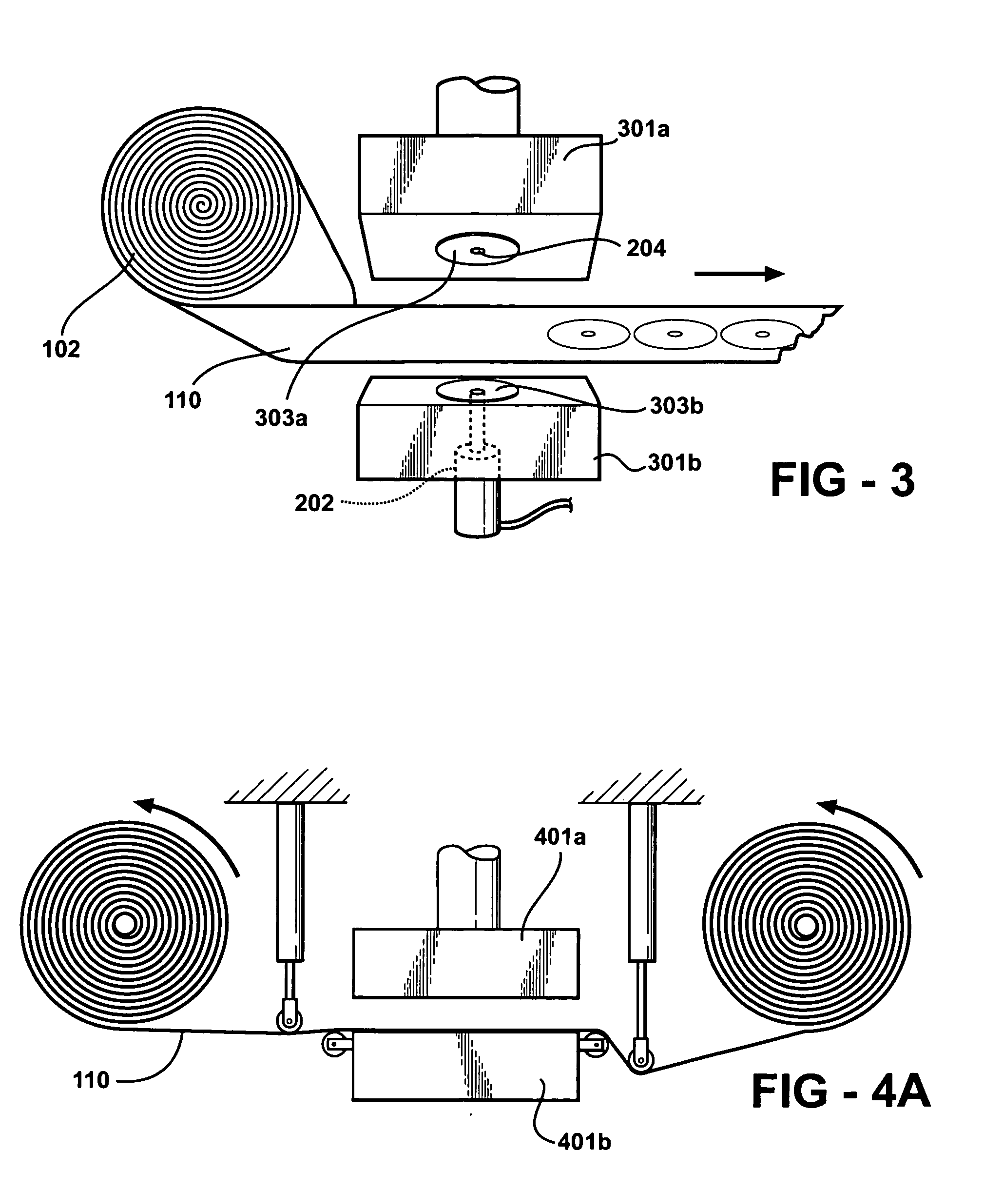
[0035] Referring now to FIG. 1, depicted therein is a device for forming optical memory in accordance with the present invention. The device includes a web payoff device, or simply a web payoff, a web path in which web material 110 travels, and a web forming apparatus disposed in the web path. The web forming apparatus includes at least one stamper 103. The stamper 103 carries at least one microform image for embossing the web 110. The stamper 103 may be supported by a platen 101a, which is supported by a carrier. The stamper may be heated by any suitable heating device. Alternative heating methods include, the use of directed energy and pressing the carrier between heated platens, electrical or oil heater, direct heating by passing electrical current through the stamper and electrical heating adjacent to the stamper. Depending on the needs of a given system, more than one stamper may be incorporated. Referring to FIGS. 1 through 3, the each stamper has a substantially flat, prefera...


PUM

PropertyMeasurementUnit
Timeaaaaaaaaaa
Thicknessaaaaaaaaaa
Speedaaaaaaaaaa

Abstract

The present invention provides a method and apparatus for the continuous manufacturing of optical memory or optical memory substrates, and/or optical disks, which includes supplying a web of material to a substrate forming apparatus, embossing a microform image onto a polymeric film, such as an information track structure for an optical device, onto one or both sides of the web with a flat stamper and punching a hole through the web during the embossing. During the embossing, the polymeric material is heated to above the glass transition temperature (Tg). A flat stamper limits the potential for warp in the web, particularly when the web is stabilized in the stamp zone. The disclosed invention is particularly useful in the production of optical disk substrates, such as polycarbonate, having a thickness of 0.6 mm or less.

Description

RELATED APPLICATION DATA [0001] The present application is filed under 35 USC § 1.53(b) as a Continuation-in-Part of U.S. patent application Ser. No. 10 / 185,246, filed on Jun. 26, 2002, which is hereby incorporated herein by reference.FIELD OF THE INVENTION [0002] The present invention relates to methods and apparatus for making optical memory. More particularly, the present invention pertains to manufacturing optical disks having pits-and-lands or grooves-and-lands pattern. Further, the present invention relates to an apparatus and method for simultaneously embossing patterns with a platen stamper on thin polymeric films for use with optical disks and punching a centered hole through the disk. BACKGROUND OF THE INVENTION [0003] Optical memory disks, such as CD (compact disks), CD-R, CD-RW; DVD (digital versatile disks), DVD-R, DVD-ROM, DVD-RAM, DVD+RW, DVD−RW, PD (phase change disks) and MO (magneto optical), etc., are typically manufactured by initially forming a substrate and the...

Claims


Application Information

Patent Timeline
IPC IPC(8): B29C35/08B29C43/02B29C59/02B29C59/04B29D17/00
CPCB29C43/00B29C43/021B29C59/026B29C59/04B29C2035/0811B29L2017/005B29C2059/023B29D17/007B29K2105/256B29L2017/00B29C2043/025
Inventor GUTMAN, GEORGEHENNESSEY, MICHAELCLARK, BARRYSTRAND, DAVID
Owner ENERGY CONVERSION DEVICES INC
Why Eureka
Try Eureka