Amplifier circuit

a technology of amplifier circuit and amplifier, which is applied in the direction of amplifier with semiconductor devices only, amplifier with semiconductor devices, amplifiers, etc., can solve the problems of reducing memory effect, increasing inter-modulation distortion products at frequencies above 20 mhz, and increasing inter-modulation distortion products at those frequencies (e.g. 100 mhz and below) may be undesirabl

Active Publication Date: 2005-04-21
NXP USA INC
View PDF5 Cites 13 Cited by
  • Summary
  • Abstract
  • Description
  • Claims
  • Application Information

AI Technical Summary

Problems solved by technology

A DC bias feed path with a low impedance line provides for lower inter-modulation distortion products and thus reduces memory effect.
One problem that may occur with circuit 101 is that the inter-modulation distortion products start to increase at frequencies above 20 MHz due to the increasing impedance

Method used


Image

  • Amplifier circuit
  • Amplifier circuit
  • Amplifier circuit

Examples


Embodiment Construction

[0015] The following sets forth a detailed description of a mode for carrying out the invention. The description is intended to be illustrative of the invention and should not be taken to be limiting.

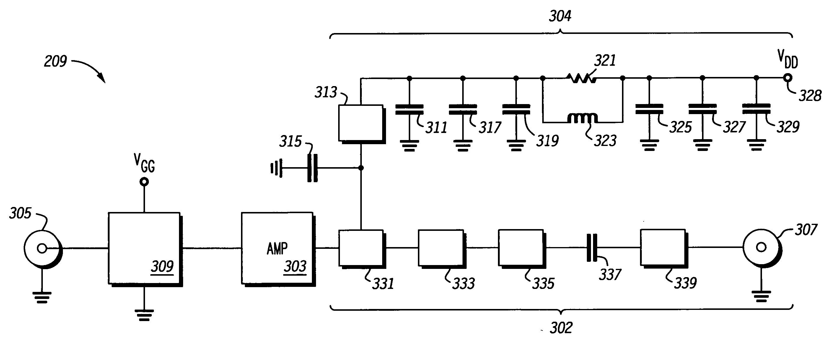
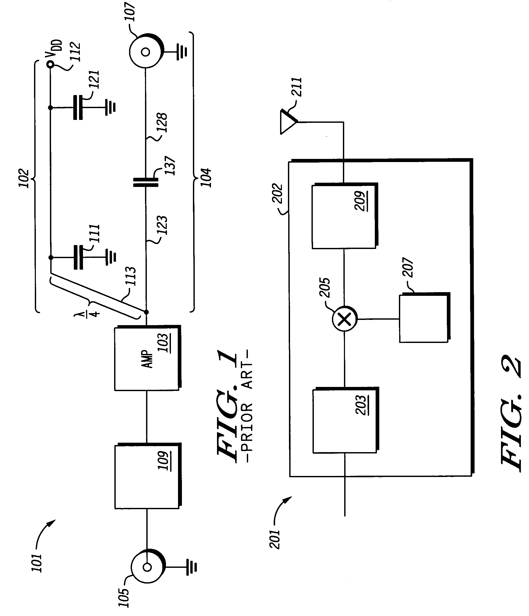
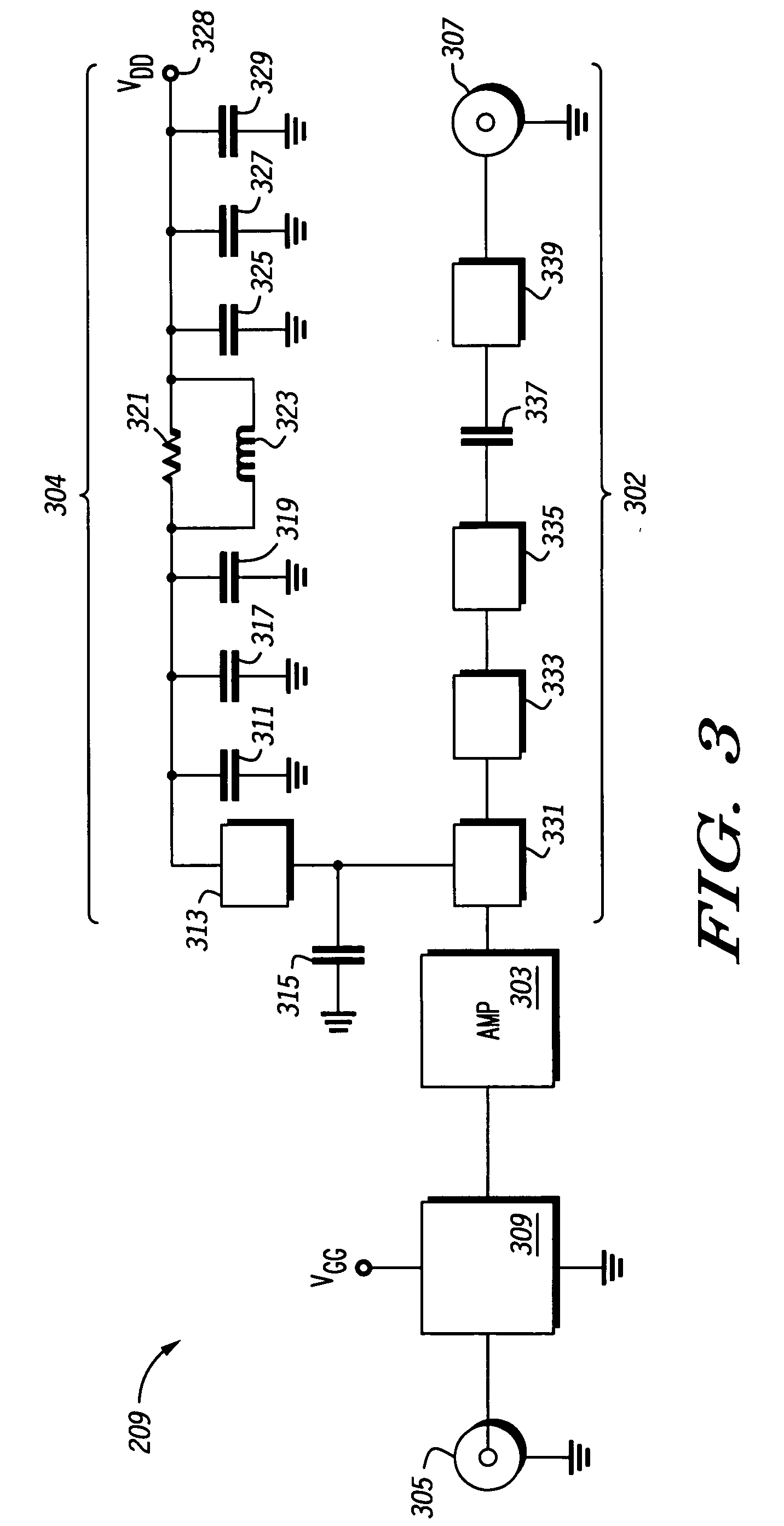
[0016]FIG. 2 shows a block diagram of a portion of a communication device according to the present invention. Communications device 201 includes a transmitter 202 and antennae 211 coupled to transmitter 202. Transmitter 202 includes an encoder 203 for providing a signal (e.g. a base band signal) containing data to a mixer 205 that modulates the signal at a carrier frequency provided to mixer 205 by oscillator 207. The output signal of mixer 205 is a modulated signal having a carrier frequency. In one embodiment, the carrier frequency is 2 GHz. In other embodiments, the carrier frequency may be at another RF frequency (10 KHz-4 GHz). Still in other embodiments, the carrier frequency may be at a different frequency (e.g. greater than the RF frequencies). The output signal of mixer 205 is...


PUM


Abstract

An amplifier circuit has an amplifier, a D.C. bias circuit, and an output signal path. The amplifier amplifies a modulated signal that has a carrier frequency. The D.C. bias circuit has a decoupling capacitor that is coupled to a transmission line having a length equal to N times the wavelength of the carrier frequency divided by four, where N is an odd integer. A low frequency decoupling capacitor is located between the decoupling capacitor and the output of the amplifier to reduce intermodulation distortion products. In one embodiment, the low frequency decoupling capacitor is a tantalum capacitor.

Description

BACKGROUND OF THE INVENTION [0001] 1. Field of the Invention [0002] This invention relates in general to amplifier circuits and more specifically to amplifier circuits with DC bias circuits. [0003] 2. Description of the Related Art [0004] Amplifiers (e.g. radio frequency (RF) amplifiers) are utilized by devices (e.g. transmitters) to amplify a signal. FIG. 1 shows an example of a prior art amplifier circuit 101 that may be located in a transmitter (not shown). Circuit 101 is located on a printed circuit board (not shown). Circuit 101 includes an amplifier 103, an input terminal 105, and an output terminal 107. Input impedance matching circuit 109 is located between input terminal 105 and amplifier 103. An output signal path 104 couples the output of amplifier 103 to output terminal 107. Path 104 includes transmission line 123, capacitor 137, and transmission line 128 which are sized to transform the impedance of the output of amplifier 103 to the impedance output terminal 107 (e.g. ...

Claims


Application Information

Patent Timeline
IPC IPC(8): H03F1/30H03F1/56H03F3/189H03F3/191
CPCH03F1/30H03F3/189H03F1/56
Inventor KAPOOR, SAMAY P.RABANY, ANTOINE J.
Owner NXP USA INC
Why Eureka
Try Eureka