

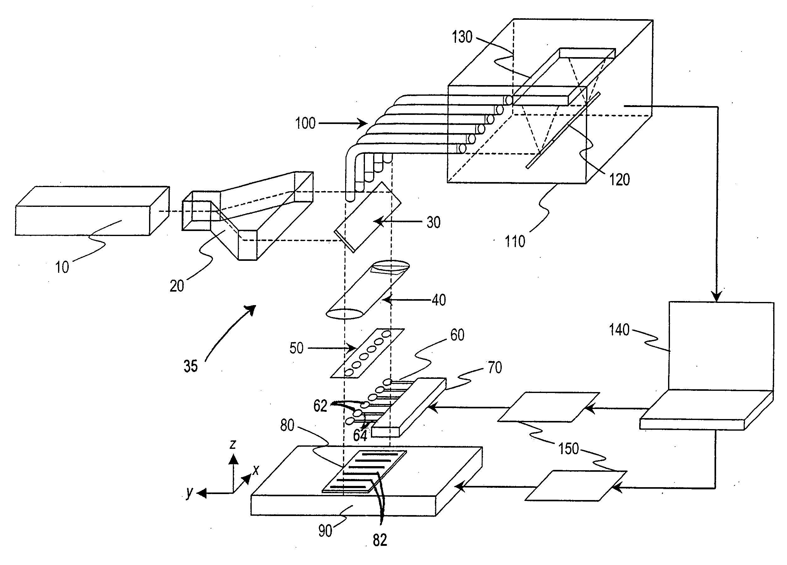
Method and apparatus for enhanced nano-spectroscopic scanning
a nano-spectroscopic scanning and nano-spectroscopic technology, applied in the field of nano-spectroscopic scanning, can solve the problems of not being able to design or operate devices, and not being able to detect specific chemical compounds or chemical groups
- Summary
- Abstract
- Description
- Claims
- Application Information
AI Technical Summary
Benefits of technology
Problems solved by technology
Method used
Image

Examples
Embodiment Construction
[0044] I. Definitions
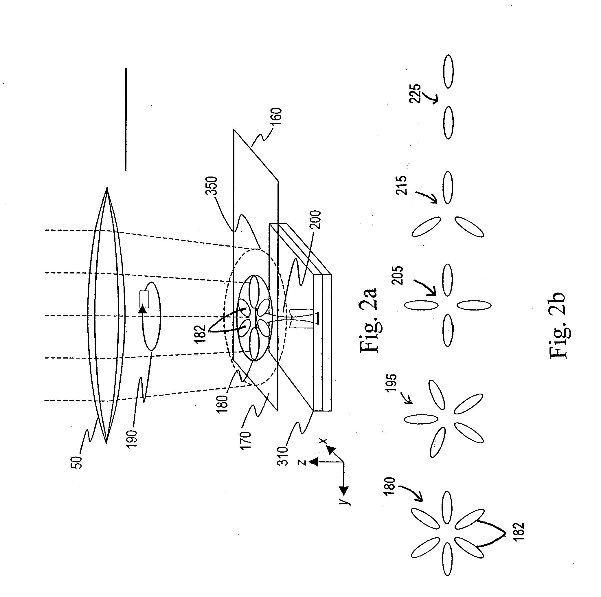
[0045] The terms below have the following meaning, unless otherwise indicated “Plasmon resonant metal” includes any metal, such as gold, silver, or aluminum which can support surface electromagnetic modes-surface plasmon polaritons (SPP), which are coupled modes of photons and plasmons.
[0046]“Chemical group” in a sample may include subunits in a polymer, or subunit moieties, such as nucleic acid bases, or chemical substituent groups, such as hydroxyl, amine, alkyl, acid, or aldehyde groups. Such chemical groups are characterized by a unique enhanced Raman spectral signatures or features.
[0047]“Gap modes” refers to electromagnetic normal modes or electromagnetic eigenmodes that are excited by external electromagnetic field in a space between two or more plasmon resonance particles and when plasmon resonance particles are placed near (less than 40 nm) from a metal surface, preferably a plasmon resonant metal surface. Examples of plasmon resonance particles are ...
PUM
| Property | Measurement | Unit |
|---|---|---|
| distance | aaaaa | aaaaa |
| distance | aaaaa | aaaaa |
| gap distance | aaaaa | aaaaa |
Abstract
Description
Claims
Application Information