Edge emitting laser with circular beam

Inactive Publication Date: 2005-04-28
IND TECH RES INST
View PDF3 Cites 6 Cited by
  • Summary
  • Abstract
  • Description
  • Claims
  • Application Information

AI Technical Summary

Benefits of technology

[0007] The invention provides a edge emitting laser with circular beam. It uses a low-carrier-mobility semiconductor compound for the light-emitting layer. The low-carrier-mobility material can greatly suppress surface recombination of the carriers. Therefore, one can form a ridge waveguide by simply etching through the light-emitting layer without the step of epitaxy growth. The invention thus provides a low-cost, high-efficiency edge emitting laser with circular beam.
[0008] The invention uses a low-carrier-mobility material to form the light-emitting layer of the edge emitting laser with circular beam. It is formed by establishing an epitaxy structure of a substrate surface. It includes, stacked from bottom to top, a bottom cladding layer, a bottom waveguide layer, a light-emitting layer, an upper waveguide layer, an upper cladding layer, and an electrode contact

Problems solved by technology

Thus, it has a very bad coupling efficiency, limiting its applications.
The light-emitting layer material used in conventional edge emitting laser with circular beams has series carrier surface recombining effects at the etching i

Method used


Image

  • Edge emitting laser with circular beam
  • Edge emitting laser with circular beam
  • Edge emitting laser with circular beam

Examples


Example

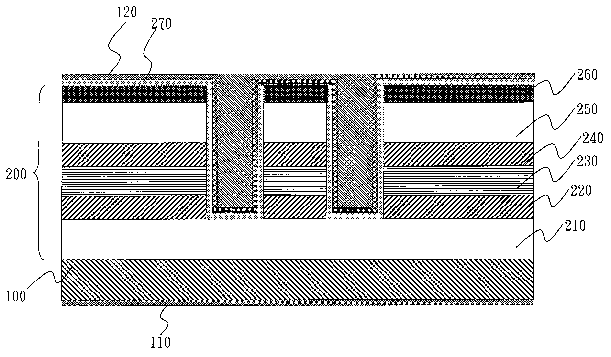
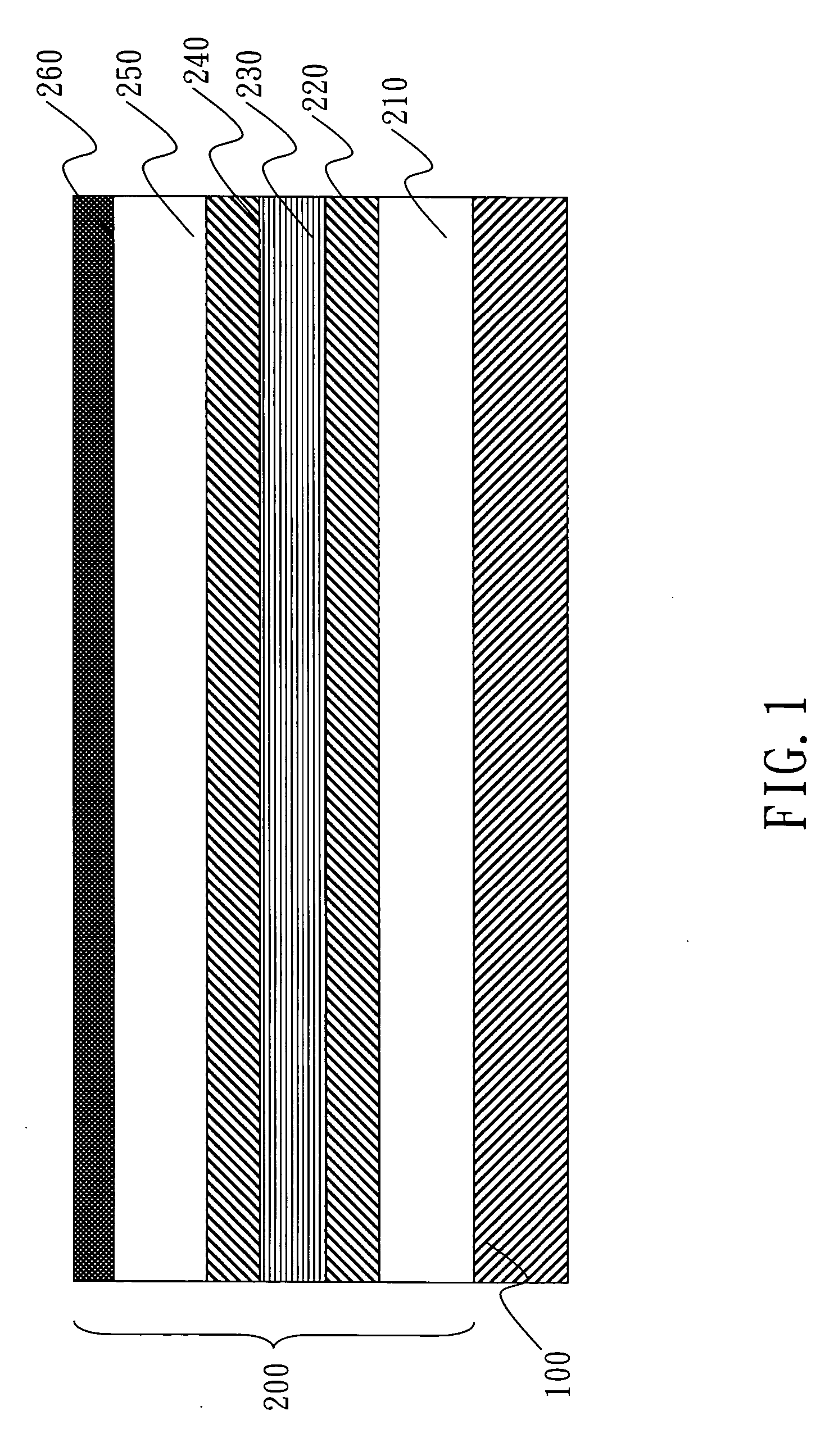
[0015] As shown in FIG. 1, the epitaxy structure 200 according to an embodiment of the invention is formed on the upper surface of a substrate 100, from bottom to top, a bottom cladding layer 210, a bottom waveguide layer 220, a light-emitting layer 230, an upper waveguide layer 240, an upper cladding layer 250, and an electrode contact layer 260. The light-emitting layer 230 is formed using the semiconductor material InvGawAl1-v-wAsxPyNzSb1-x-y-z(0

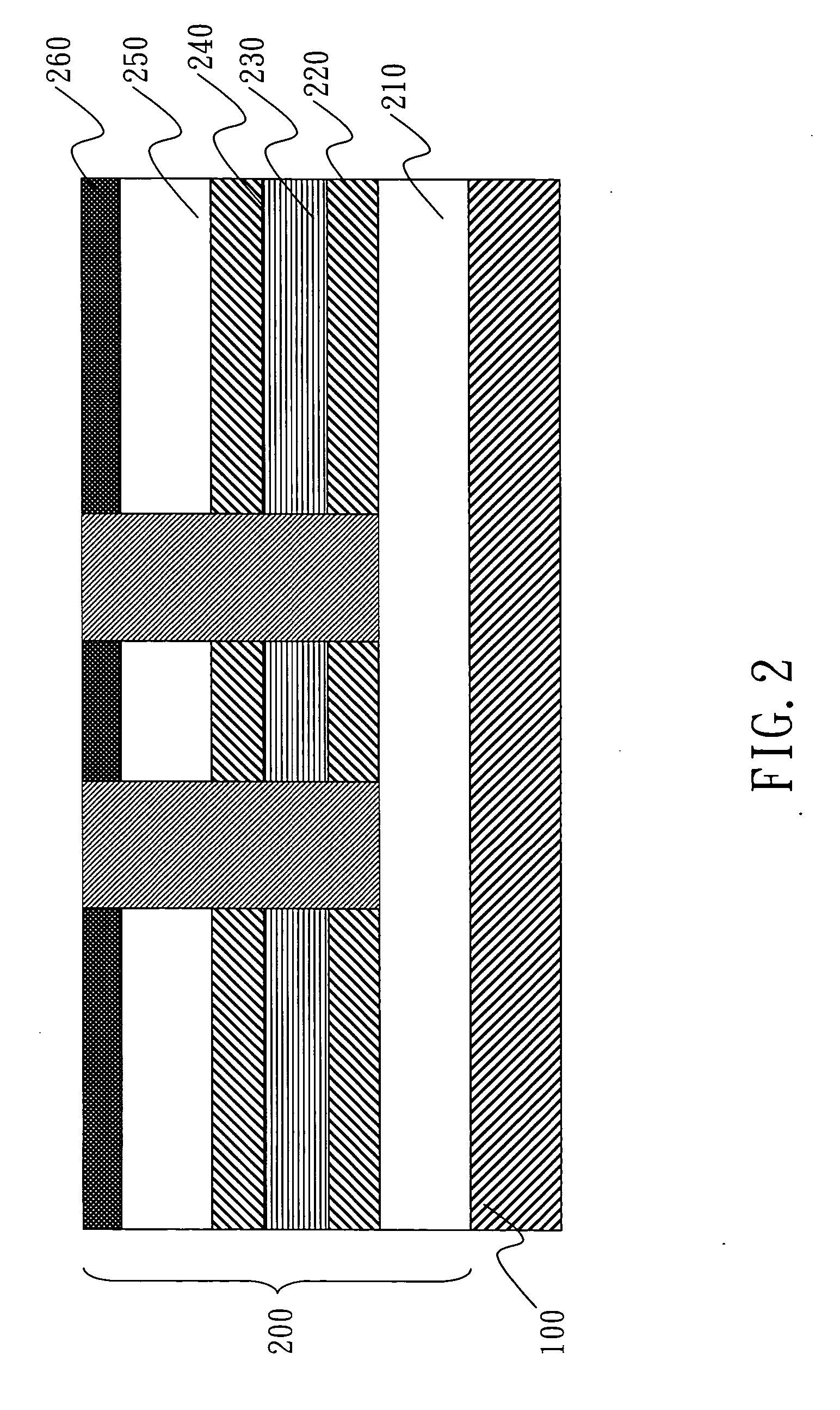
[0016] With reference to FIG. 2, combining lithography and etching techniques, the epitaxy structure is etched to form a groove through the light-emitting layer 230. Etching starts from the surface of the epitaxy structure 200 through the light-emitting layer 230 to form a ridge waveguide.

[0017] With reference to FIG. 3, a passivation dielectric layer 270 is formed on the surface of the epitaxy structure 200. The ridge waveguide region of the dielectric layer 270 is exposed by etching. A P-typ...


PUM


Abstract

An edge emitting laser with circular beam using a low-carrier-mobility diluted nitride semiconductor material for an epitaxy light-emitting layer is disclosed. The low-carrier-mobility material can greatly suppress surface recombination of carriers. The epitaxy structure established on the substrate surface includes, from bottom to top, a bottom cladding layer, a bottom waveguide layer, a light-emitting layer, an upper waveguide layer, an upper cladding layer, and an electrode contact layer. The light-emitting layer is formed from a diluted nitride material. Etching is performed from the epitaxy structure through the light-emitting layer, forming a ridge waveguide that has a large reflective index difference between the light-emitting layer and the dielectric passivation layer.

Description

BACKGROUND OF THE INVENTION [0001] 1. Field of Invention [0002] The invention relates to an edge emitting laser and, in particular, to a edge emitting laser with circular beam that uses a low-carrier-mobility material. [0003] 2. Related Art [0004] Semiconductor lasers have the features of compact sizes, long lifetime, good vibration tolerance, being highly directional, and large output power. They are ideal for the light sources of long-distance, large-capacity communications and high-density recording media. Currently, most of their applications are in optical communications and storage industries. Therefore, the semiconductor lasers have a brighter future. [0005] According to their structures and light-emitting position, the semiconductor lasers are divided into surface-emitting lasers and edge emitting lasers. The cavity of the edge emitting laser is parallel to the epitaxy layer. The reflecting surface is formed by coating a reflecting film on the cutting surface of a crystal. I...

Claims


Application Information

Patent Timeline
IPC IPC(8): H01S5/22H01S5/00H01S5/20H01S5/227H01S5/323
CPCH01S5/2086H01S5/2222H01S2301/18H01S5/2275H01S5/32366H01S5/227
Inventor WANG, JYH-SHYANGLIN, GRAYKOVSH, ALEXEY R.LIVSHITS, D. A.
Owner IND TECH RES INST
Why Eureka
Try Eureka