Process for producing oxide films

a technology of oxide film and bismuth, which is applied in the manufacture of cables/conductors, ceramics, chemical vapor deposition coatings, etc., can solve the problems of not being able to achieve the desired bisub>, not having to find appropriate bismuth — oxygen source combinations, and not having to strictly control the substrate temperature and dosage control, etc., to achieve good thin film properties, excellent conformality, and excellent and automatic self-control of film growth

Active Publication Date: 2005-04-28
ASM INTERNATIONAL
View PDF5 Cites 71 Cited by
  • Summary
  • Abstract
  • Description
  • Claims
  • Application Information

AI Technical Summary

Benefits of technology

[0010] It is an object of preferred embodiments of the invention to reduce the problems of the prior art and to provide a novel ALD process for producing bismuth-containing oxide thin films.
[0020] Considerable advantages are obtained by the preferred embodiments. Thus, the novel ALD source materials, exemplified by tris(bis(trialkylsilyl)amido) bismuth(III), have been tested and found to work well as precursors for both binary and multicomponent oxides of bismuth. The properties of this novel precursor group are illustrated below by tris(bis(trimethylsilyl)-amido)bismuth(III)[in the following abbreviated Bi(btsa)3]. Bi(btsa)3 is a volatile compound, which is stable at a temperature range compatible with ranges used for the ALD deposition using precursors of many other metal components in bismuth-containing multi-component oxide materials. Therefore, the preferred embodiments make it possible to deposit thin films by ALD, while operating the process at conditions under which Bi(btsa)3 is stable.
[0021] Films deposited by a preferred embodiment exhibit good thin films properties, e.g., they have excellent conformality even on uneven surfaces. As a result, the novel films can be used in 3-D folding and / or roughened capacitors. The invention also provides for excellent and automatic self-control of film growth.

Problems solved by technology

Advantageously, ALD requires neither strict temperature control of the substrates nor precise dosage control of source chemicals.
The main problem has been finding appropriate bismuth —oxygen source combinations for depositing bismuth oxide.
However, the levels were too low for forming the desired Bi4Ti3O12 phase.
As the above surveys show, there are no satisfactory processes known for producing bismuth-containing ferroelectric films by the Atomic Layer Deposition technique.

Method used


Image

  • Process for producing oxide films
  • Process for producing oxide films
  • Process for producing oxide films

Examples


example 1

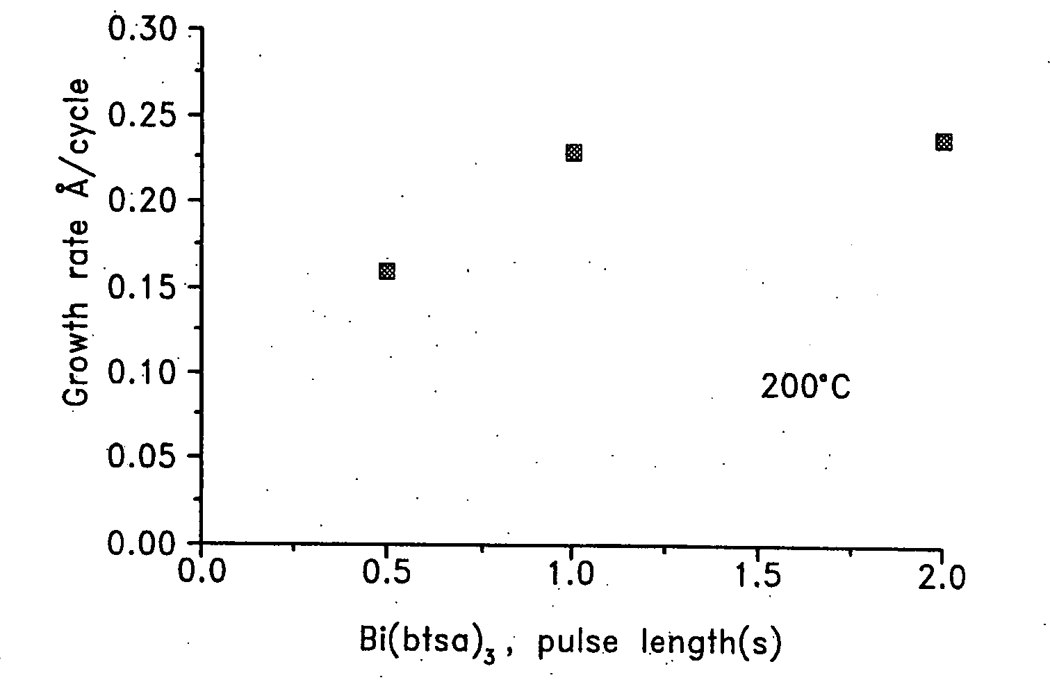
[0064] ALD Growth of Bi2O3 from Bi(btsa)3 and H2O was carried out at temperatures in the range of from 150 to 200° C. At deposition temperatures of 225° C. and above, no significant growth was observed, probably due to precursor decomposition. At 200° C. the Bi—O growth rate saturates at 0.23 Å / cycle (FIG. 1).

example 2

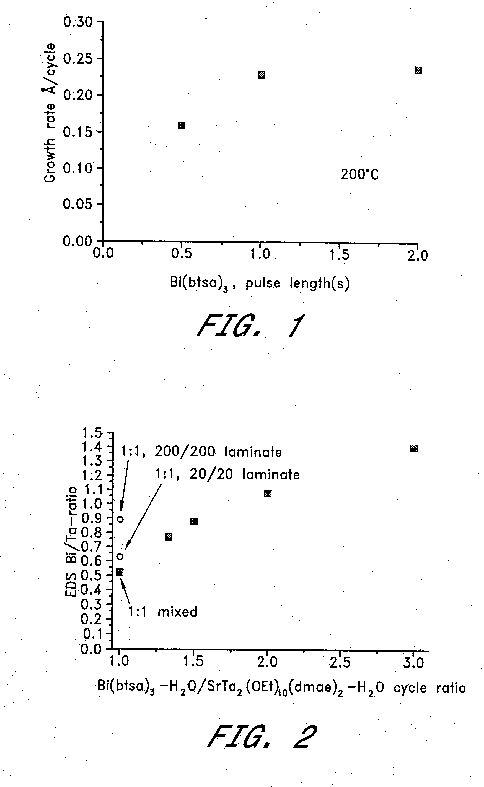
[0065] SrBi2Ta2O9 films were deposited at 200° C. by mixing [Bi(btsa)3—H2O and [SrTa2(OEt)10(dmae)2—H2O] cycles (FIG. 2). Average growth rates were roughly 0.2 Å / cycle. At a 2:1 cycle mixing ratio, films were obtained having 8 atomic percentage Bi in excess of stoichiometric. This composition is suitable for ferroelectric applications.

example 3

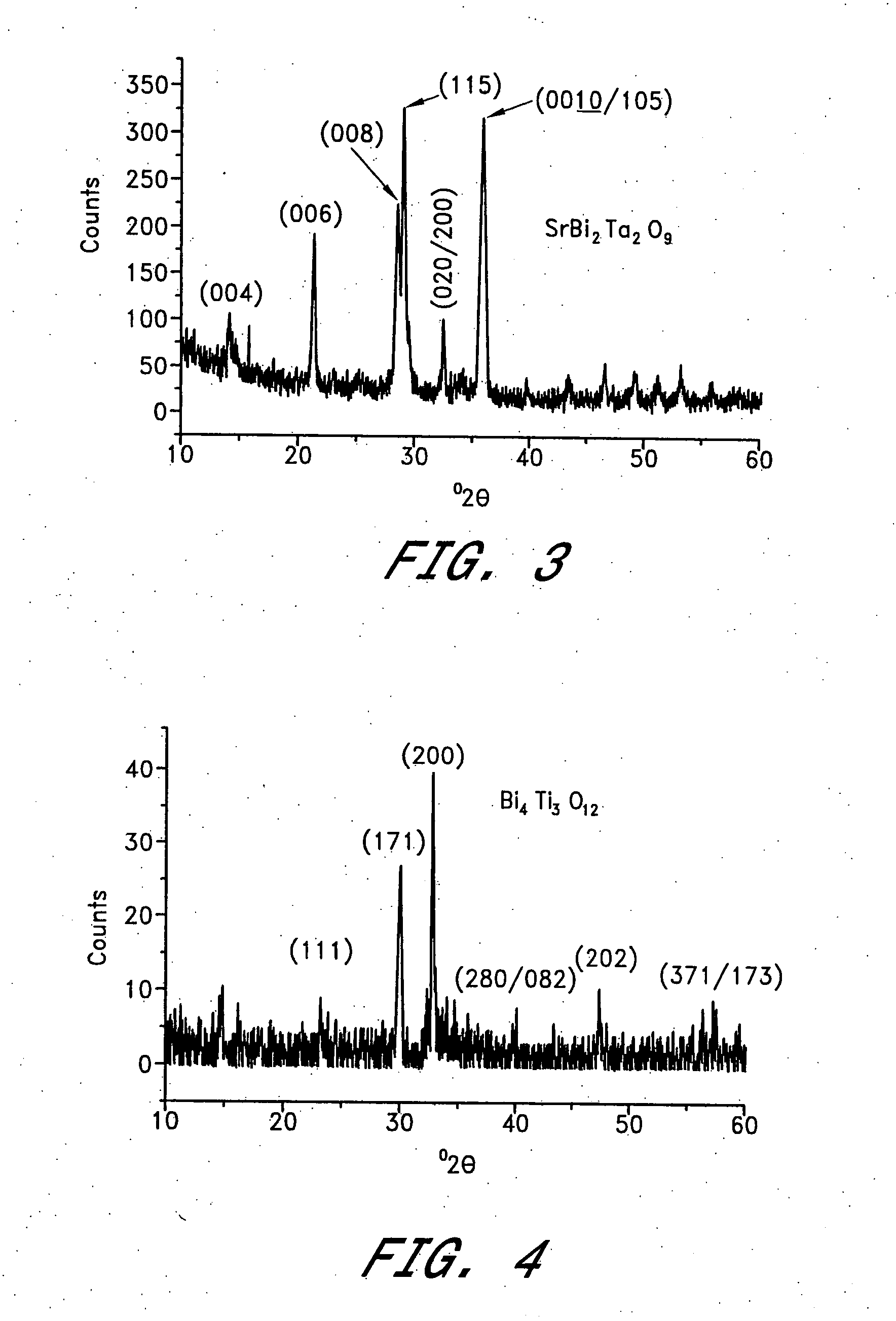
[0066] A second approach was also used for depositing SrBi2Ta2O9. Thus, amorphous laminate layers of Sr—Ta—O and Bi—O were grown. In this case, the overall composition was adjusted by varying the thicknesses of these layers, and the desired compound was formed by reacting the layers with each other in the following annealing steps. All the as-deposited SBT films were amorphous, but after annealing in air at 750° C. the desired ferroelectric phase was observed (FIG. 3).


PUM

PropertyMeasurementUnit
temperatureaaaaaaaaaa
temperaturesaaaaaaaaaa

Abstract

A process for producing bismuth-containing oxide thin films by Atomic Layer Deposition, including using an organic bismuth compound having at least one silylamido ligand as a source material for the bismuth oxide. Bismuth-containing oxide thin films produced by the preferred embodiments can be used, for example, as ferroelectric or dielectric material in integrated circuits and / or as superconductor materials.

Description

BACKGROUND OF THE INVENTION [0001] 1. Field of the Invention [0002] The invention generally relates to bismuth-containing oxide films. In particular, the present invention relates to a process for manufacturing bismuth-containing oxide thin films by Atomic Layer Deposition (ALD). [0003] 2. Description of the Related Art [0004] Bismuth is a component of several technologically important binary and multicomponent oxide thin film materials, particularly the ferroelectric oxides Bi4Ti3O12, (Bi,La)4Ti3O12, and SrBi2Ta2O9 and, also, the superconducting oxide Bi2Sr2CaCu2O8+x. Ferroelectric bismuth oxide films have great potential use in ferroelectric memory cells. In such uses, the films are likely to be formed with capacitors in the form of 3-D structures, which means that good conformality of the ferroelectric film is desired to ensure proper function of the memory cell. [0005] Atomic Layer Deposition, in the following also abbreviated “ALD”, is a deposition method in which a product, su...

Claims


Application Information

Patent Timeline
Patent Type & Authority Applications(United States)
IPC IPC(8): C07F9/94C23C16/00C23C16/40C23C16/455H01B3/12H01B13/00H01L21/316H01L21/8246H01L27/105
CPCC07F9/94C23C16/40C23C16/45553C23C16/45525C23C16/45531C23C16/407
Inventor VEHKAMAKI, MARKOHATANPAA, TIMORITALA, MIKKOLESKELA, MARKKU
Owner ASM INTERNATIONAL
Why Eureka
Try Eureka