Method to improve post wafer etch cleaning process

a technology of cleaning process and semiconductor process, applied in drying machines, lighting and heating apparatus, furnaces, etc., can solve the problems of device degradation, semiconductor process wafer rejection, and increase the detrimental effect of particulate contamination

Inactive Publication Date: 2005-05-05
TAIWAN SEMICON MFG CO LTD
View PDF5 Cites 26 Cited by
  • Summary
  • Abstract
  • Description
  • Claims
  • Application Information

AI Technical Summary

Problems solved by technology

A critical condition in semiconductor manufacturing is the absence of particulates on the wafer processing surface, since microscopic particles may interfere with and adversely affect subsequent processing steps leading to device degradation and ultimately semiconductor process wafer rejection.
For example, as semiconductor feature sizes decrease, the detrimental affect of particulate contamination increases, requiring removal of ever smaller particles.
For example, particles as small as 5 nm are no longer acceptable in many nano-integrated circuit manufacturing processes.
Subsequent processes, including dielectric or metal deposition processes may be detrimentally affected by the presence of water, including causing inadequate adhesion of the overlying layer.
One problem with prior art solvent vapor drying processes is that the efficiency of the drying process is frequently unpredictable due to variation is the concentration of solvent in the solvent vapor.
For example, prior art vapor drying processes have limited temperature control capabilities where temperature variations can impact the steady state concentration of solvent vapor delivered to the wafer surface.
In addition, prior art processes including prior temperature control have proved insufficient in maintaining a sufficiently high solvent vapor concentration during wafer drying including high aspect ratio semiconductor features.
Temperature variations within the wafer drying space and along the vapor supply lines can result in inconsistent and inadequate solvent vapor concentrations.
As a result, wafer yields are lowered as a result of defects caused by an incompletely dry wafer surface as well as requiring unnecessarily extended drying times to ensure complete wafer drying.

Method used


Image

  • Method to improve post wafer etch cleaning process
  • Method to improve post wafer etch cleaning process
  • Method to improve post wafer etch cleaning process

Examples


Embodiment Construction

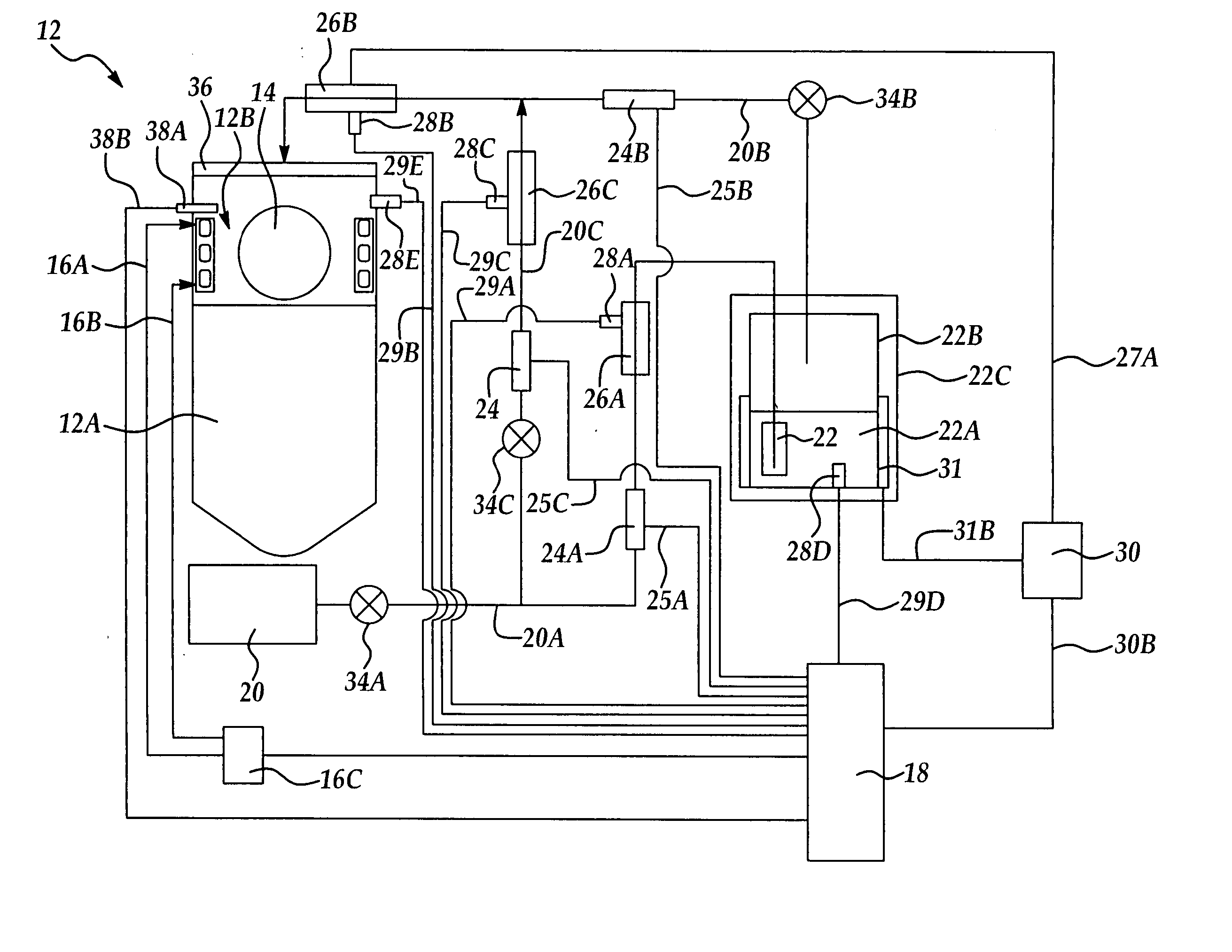
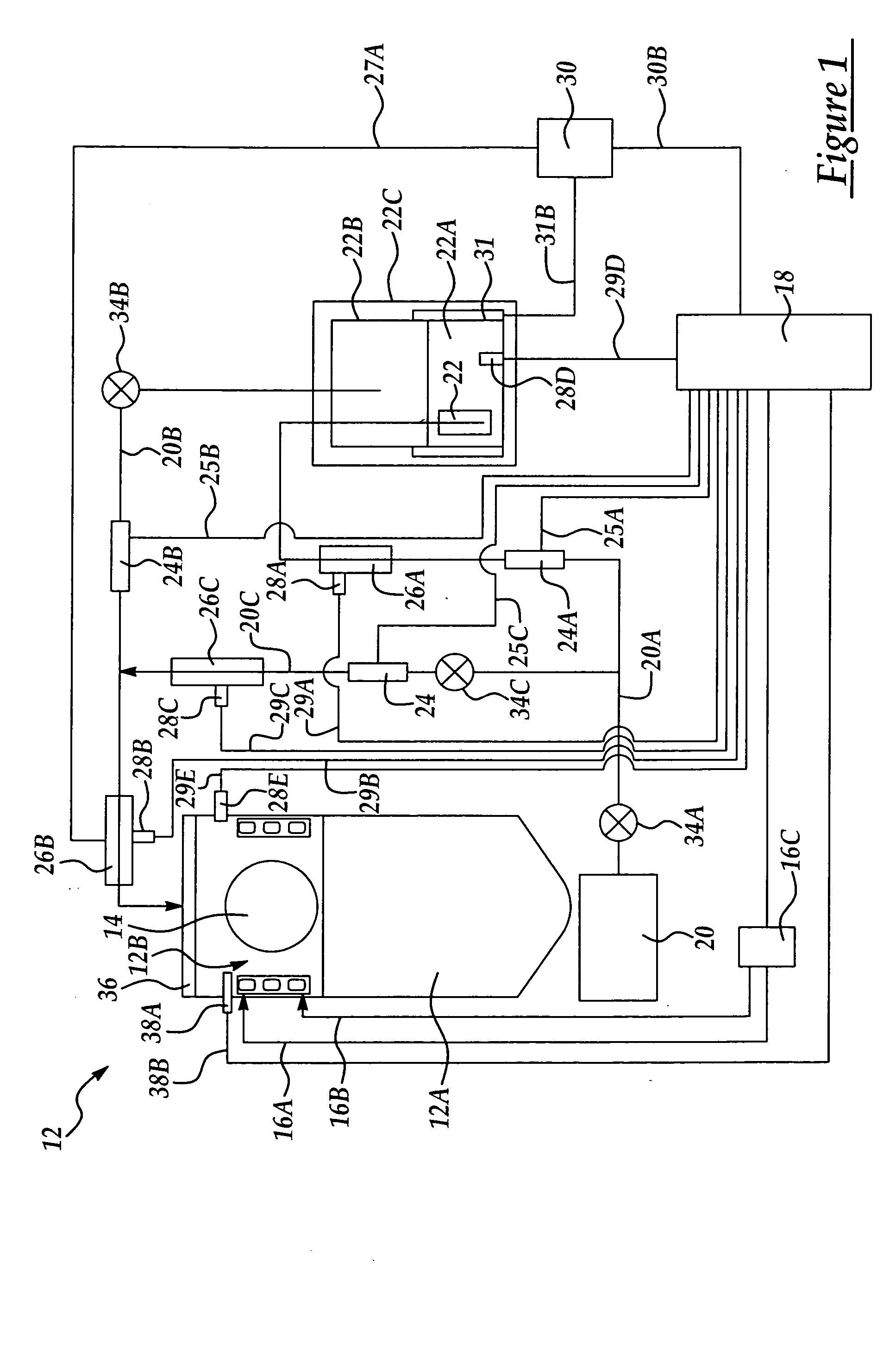
[0016] The present invention is directed at a solvent vapor drying process and apparatus, preferably using alcohol, for example, isopropyl (IPA) as the solvent, for removing water from a semiconductor process wafer surface following a deionized water rinsing process. While the method and apparatus of the present invention is explained with reference to a Marangoni type drying process, it will be appreciated that the method of and apparatus of the present invention may be used in other vapor drying processes including a static wafer drying process where the wafer is held in a static position in a vapor drying chamber following a rinsing process.

[0017] In addition, the method and apparatus of the present invention are particularly suitable for removing water from a wafer process surface following formation of vias in a dielectric insulating layer, preferably with a via diameter less than about 0.25 microns and an aspect ratio (depth to diameter) of greater than about 5. The method an...


PUM


Abstract

A method and apparatus for performing a semiconductor process wafer drying process, the method provides a semiconductor wafer having a process surface disposed in an enclosed drying space following exposure of the process surface to water; supplying a solvent vapor to the drying space at a predetermined concentration from a solvent vapor source and at least one solvent vapor supply line; determining at least one of a solvent vapor concentration and a solvent vapor temperature in the drying space; and heating in response to the determined solvent concentration at least one of at least a portion of one of the solvent vapor source, the at least one solvent vapor supply line, and at the drying space to alter the solvent vapor concentration in the drying space.

Description

FIELD OF THE INVENTION [0001] This invention generally relates to semiconductor wafer manufacturing and more particularly to a method for vapor drying semiconductor process wafers following an anisotropic plasma assisted etch process and a rinsing process. BACKGROUND OF THE INVENTION [0002] In creating a multiple layer (level) semiconductor devices on a semiconductor wafer, each layer making up the device may be subjected to one or more deposition processes, for example using chemical vapor deposition (CVD) or physical vapor deposition (PVD) and usually including one or more dry etching processes. A critical condition in semiconductor manufacturing is the absence of particulates on the wafer processing surface, since microscopic particles may interfere with and adversely affect subsequent processing steps leading to device degradation and ultimately semiconductor process wafer rejection. [0003] While the wafer cleaning process has been always been a critical step in the semiconducto...

Claims


Application Information

Patent Timeline
Patent Type & Authority Applications(United States)
IPC IPC(8): H01L21/00H01L21/306
CPCH01L21/67034H01L21/02063
Inventor CHEN, JIA-RENSHIU, L.D.KUOC, C.C.TSAI, H.H.
Owner TAIWAN SEMICON MFG CO LTD
Why Eureka
Try Eureka