Optically functional layer, method of forming optically functional layer, and liquid crystal display element

a technology liquid crystal displays, which is applied in the direction of polarizing elements, instruments, transportation and packaging, etc., can solve the problems of insufficient heat resistance of optically functional layers obtained by using any of the above photopolymerization initiators, risk of deteriorating a display quality level, and insufficient chemical resistance, so as to improve the orientation of layers and reduce the risk of deterioration , the effect of heat resistan

Active Publication Date: 2005-05-05
DAI NIPPON PRINTING CO LTD
View PDF12 Cites 17 Cited by
  • Summary
  • Abstract
  • Description
  • Claims
  • Application Information

AI Technical Summary

Benefits of technology

[0032] According to the ninth aspect of the present invention, after development, heating is performed at a specific range of temperature, thereby, a method of forming an optically functional layer which can more stabilize the orientation of layer can be provided besides the effect of the seventh aspect of the present invention.
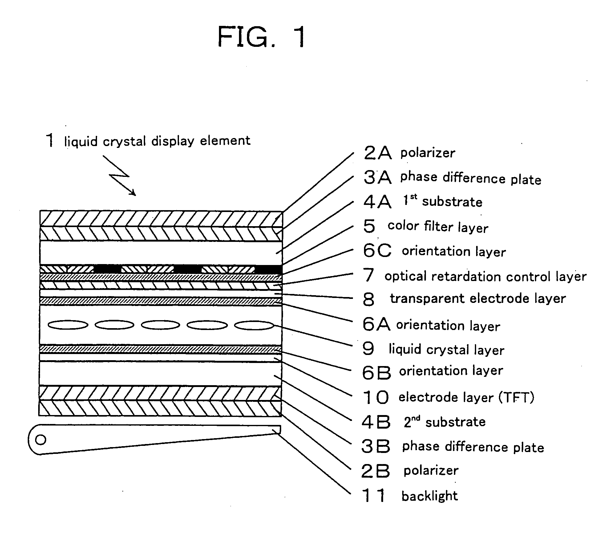
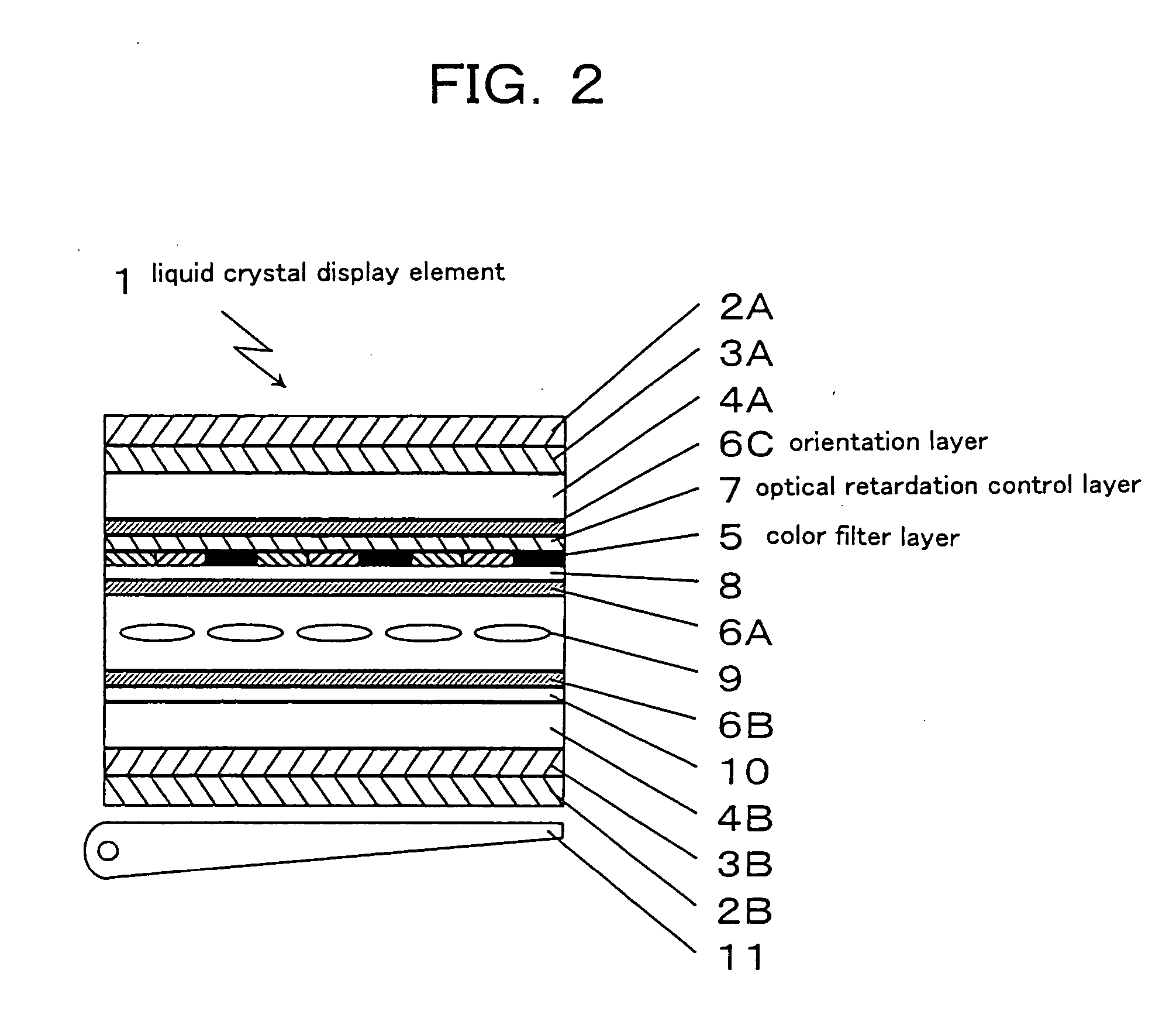
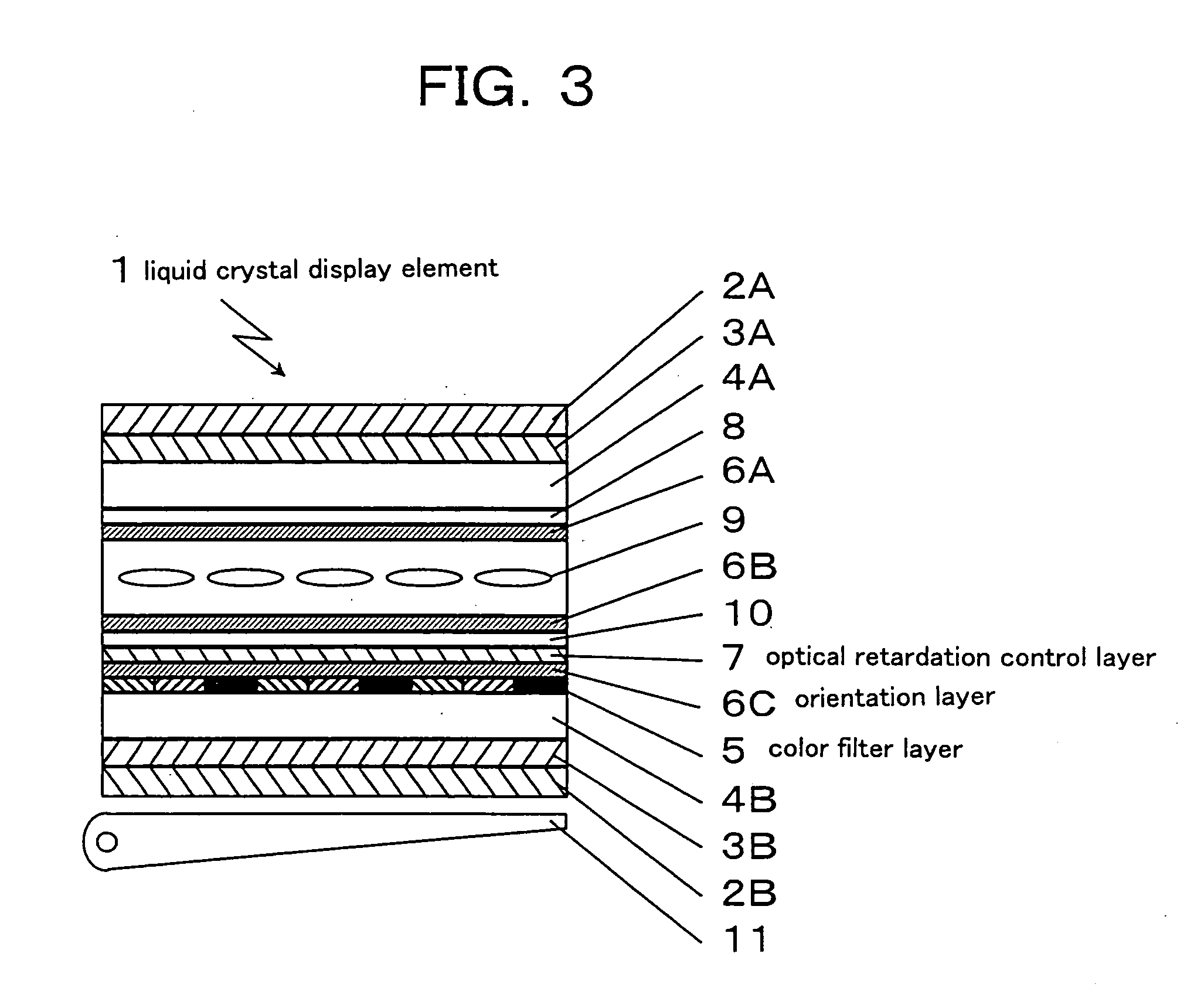
[0033] According to the tenth aspect of the present invention, the optically functional layer of the first or second aspect of the present invention (particularly, an optical retardation control layer) is laminated inside of a cell, thereby, a liquid crystal display element wherein the durability such as heat resistance, chemical resistance or the like of the optically functional layer is improved can be provided.
[0034] According to the eleventh aspect of the present invention, a color filter layer is laminated, thereby, a liquid crystal display element wherein a color display is capable can be provided besides the effect of the tenth aspect of the present invention.
[0035] According to the twelfth aspect of the present invention, a liquid crystal display element which can provide plural function of optically functional layers can be provided besides the effect of the tenth to eleventh aspect of the present invention.
[0036] According to the thirteenth aspect of the present invention, a liquid crystal display element which can sufficiently exhibit each function of two optically functional layers can be provided besides the effect of the twelfth aspect of the present invention.
[0037] According to the fourteenth aspect of the present invention, a liquid crystal display element wherein there is no blur in boundary of a transparent portion and the function of each optically functional layer is conjugated can be provided besides the effect of the thirteenth aspect of the present invention.

Problems solved by technology

However, the heat resistance of the optically functional layers obtained by using any of the above photopolymerization initiators was not necessarily sufficient.
Particularly, there was a risk of deteriorating a display quality level as impurity elutes into a liquid crystal layer when an optical retardation control layer comes into contact with the liquid crystal layer because of the insufficient heat resistance of the optical retardation control layer leading to the deterioration in the optical retardation control layer due to high temperature of processing after forming the optical retardation control layer, the insufficient chemical resistance of the obtained optical retardation control layer, or the like.

Method used


Image

  • Optically functional layer, method of forming optically functional layer, and liquid crystal display element
  • Optically functional layer, method of forming optically functional layer, and liquid crystal display element
  • Optically functional layer, method of forming optically functional layer, and liquid crystal display element

Examples


example 1

[0080] As composition for forming retardation layer, each component of the following composition was mixed and solved to prepare and used for spin coating on a glass substrate with an orientation layer having rubbing treatment. After removing a solvent, the coating layer after orientation treatment was subject to ultraviolet irradiation for photopolymerization at room temperature in the air with the use of ultra-high-pressure mercury-vapor lamp (output: 20 mW / cm2, wavelength: 365 nm) under the condition of radiating amount of 1000 mJ / cm2. As the result, the thickness of the obtained retardation layer was 1.03 μm, and retardation was 143 nm measured with a colorimetric light at wavelength of 589 nm.

[0081] Further, the obtained retardation layer was subject to curing treatment in a clean oven under condition of temperature of 230° C. and time of 1 hour, a retardation layer having slow axes in in-plain direction of layer was obtained. The thickness of the retardation layer after the c...

example 2

[0083] Except that a photopolymerization initiator represented by the Formula (2) was used as a photopolymerization initiator, a retardation layer was obtained with the compounding ratio of the composition for forming a retardation layer and the forming condition or the like similar to Example 1. The thickness of the obtained retardation layer after photopolymerization by ultraviolet irradiation was 1.02 μm and retardation was 132 nm when measured with a colorimetric light at wavelength of 589 nm.

[0084] The obtained retardation layer was further subject to curing treatment in a clean oven under condition of temperature of 230° C. and time of 1 hour, and a retardation layer having slow axes in in-plain direction of layer was obtained. The thickness of the retardation layer after curing treatment was 0.96 μm, and retardation was 119 nm when measured with a colorimetric light at wavelength of 589 nm.

example 3

[0085] Except that the coating layer after orientation treatment was subject to ultraviolet irradiation at 60° C. and photopolymerization, a retardation layer was obtained similarly as in Example 2. The thickness of the retardation layer obtained by photopolymerization by ultraviolet irradiation was 1.05 μm, and retardation was 122 nm when measured with a colorimetric light at wavelength of 589 nm.

[0086] The obtained retardation layer was further subject to curing treatment in a clean oven under condition of temperature of 230° C. and time of 1 hour. The thickness of the retardation layer was 1.03 μm, and retardation was 119 nm when measured with a colorimetric light at wavelength of 589 nm. The difference between the measured value and the retardation value after photopolymerization was small.


PUM

PropertyMeasurementUnit
selective reflection wavelengthaaaaaaaaaa
thicknessaaaaaaaaaa
thicknessaaaaaaaaaa

Abstract

The present invention is to solve a problem that, conventionally, there is a risk of impurity elution when the optical retardation control layer obtainable by photopolymerization comes into contact with the liquid crystal layer because of the deterioration in heat resistance of the optical retardation control layer due to high temperature of post-process, the insufficient chemical resistance or the like. α-amino alkylphenone based 2-methyl-1[4-(methylthio)phenyl]-2-morpholinopropane-1-one or 2-benzyl-2-dimethylamino-1-(4-morpholinophenyl)-butanone-1 are used as a photopolymerization initiator to be compounded in a composition for forming an optical retardation control layer or other optically functional layers.

Description

BACKGROUND OF THE INVENTION [0001] 1. Field of the Invention [0002] The present invention relates to an optically functional layer comprising a cured product of polymerizable liquid crystal composition by polymerization such as an optical retardation control layer, a color filter layer, a polarizing control layer or the like, which is particularly suitable for applying to various displays, notably, a liquid crystal display. [0003] The present invention also relates to a method of forming the optically functional layer, and a liquid crystal display element using the optically functional layer. [0004] 2. Description of the Related Art [0005] In order to form an optically functional layer such as the above mentioned optical retardation control layer or the like using a polymerizable liquid crystal composition, it is necessary to employ a method comprising steps of applying a polymerizable liquid crystal composition on a substrate and subjecting the applied substrate to exposure to cure...

Claims


Application Information

Patent Timeline
Patent Type & Authority Applications(United States)
IPC IPC(8): G02B5/20C09K19/38C09K19/52C09K19/54G02B5/30G02F1/13363
CPCC09K19/38C09K19/52C09K19/54C09K2019/528C09K2219/03G02B5/3016Y10T428/1059G02F2001/133565G02F2001/133633G02F2413/03Y10T428/10Y10T428/1036G02F1/13363C09K2323/00C09K2323/03C09K2323/05G02F1/133565G02F1/133633
Inventor ISHIZAKI, KOUJIMORIYA, NORIHISAISHIKAWA, YUKIKO YI
Owner DAI NIPPON PRINTING CO LTD
Why Eureka
Try Eureka