Photodiode sensor and pixel sensor cell for use in an imaging device

a technology of pixel sensor and imaging device, which is applied in the direction of radiation control device, solid-state device, semiconductor device, etc., can solve the problems of high power dissipation of large arrays, ccd imagers also suffer from a number, and can not be used in large arrays. , to achieve the effect of improving dynamic range, increasing surface area, and increasing charge capacity

Inactive Publication Date: 2005-05-05
APTINA IMAGING CORP
View PDF29 Cites 25 Cited by
  • Summary
  • Abstract
  • Description
  • Claims
  • Application Information

AI Technical Summary

Benefits of technology

[0031] The multi-trench photosensor provides the photosensitive element with an increased surface area compared to a flat photosensor occupying a comparable area on a substrate. The multi-trench photosensor also exhibits a higher charge capacity, improved dynamic range, and a better signal-to-noise ratio.

Problems solved by technology

However, CCD imagers also suffer from a number of disadvantages.
For example, they are susceptible to radiation damage, they exhibit destructive read out over time, they require good light shielding to avoid image smear and they have a high power dissipation for large arrays.
Additionally, while offering high performance, CCD arrays are difficult to integrate with CMOS processing in part due to a different processing technology and to their high capacitances, complicating the integration of on-chip drive and signal processing electronics with the CCD array.
While there has been some attempts to integrate on-chip signal processing with the CCD array, these attempts have not been entirely successful.
CCDs may also suffer from incomplete charge transfer from pixel to pixel during charge transfer which also results in image smear.
There are drawbacks, however, with prior CMOS imagers.
Prior CMOS pixel photosensors suffer dynamic range and charge capacity limitations, and undesirably low signal-to-noise ratios.
These methods add process complexity, may limit the use of advantageous features such as silicided gates, and may result in increased pixel cell sizes, thereby reducing pixel array densities.

Method used


Image

  • Photodiode sensor and pixel sensor cell for use in an imaging device
  • Photodiode sensor and pixel sensor cell for use in an imaging device
  • Photodiode sensor and pixel sensor cell for use in an imaging device

Examples


Embodiment Construction

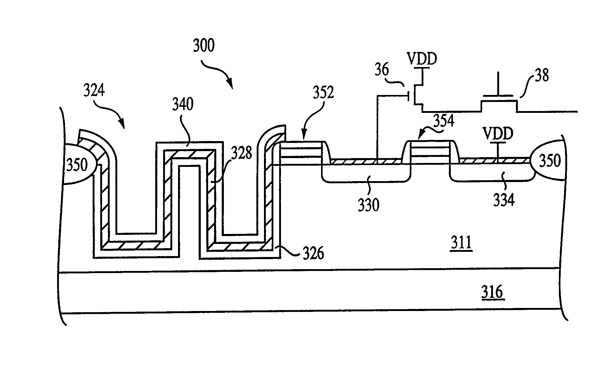
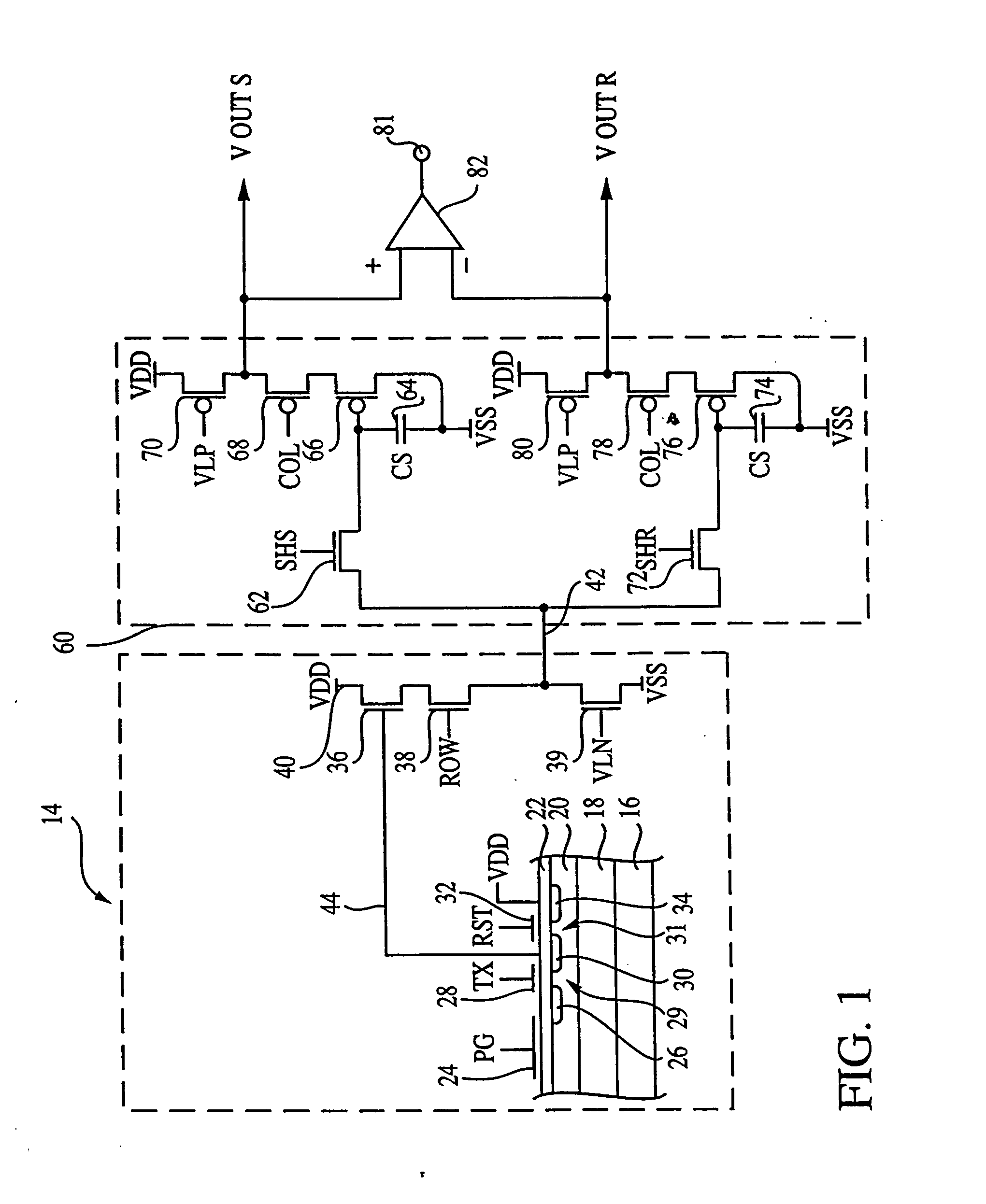
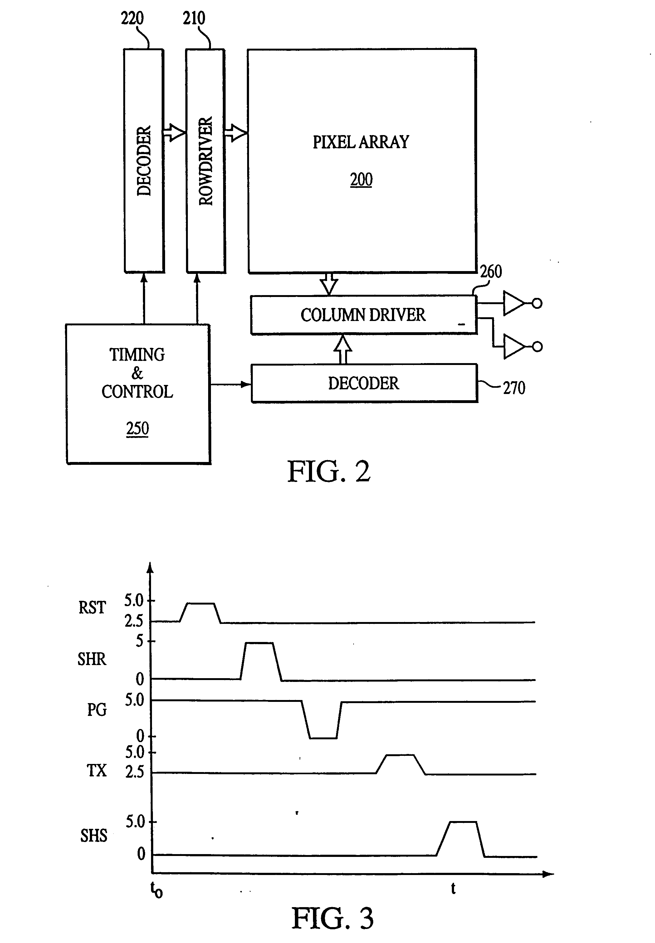
[0048] In the following detailed description, reference is made to the accompanying drawings which form a part hereof, and in which is shown by way of illustration specific embodiments in which the invention may be practiced. These embodiments are described in sufficient detail to enable those skilled in the art to practice the invention, and it is to be understood that other embodiments may be utilized, and that structural, logical and electrical changes may be made without departing from the spirit and scope of the present invention.

[0049] The terms “wafer” and “substrate” are to be understood as including silicon-on-insulator (SOI) or silicon-on-sapphire (SOS) technology, doped and undoped semiconductors, epitaxial layers of silicon supported by a base semiconductor foundation, and other semiconductor structures. Furthermore, when reference is made to a “wafer” or “substrate” in the following description, previous process steps may have been utilized to form regions or junctions...


PUM


Abstract

A multiple-trench photosensor for use in a CMOS imager having an improved charge capacity. The multi-trench photosensor may be either a photogate or photodiode structure. The multi-trench photosensor provides the photosensitive element with an increased surface area compared to a flat photosensor occupying a comparable area on a substrate. The multi-trench photosensor also exhibits a higher charge capacity, improved dynamic range, and a better signal-to-noise ratio. Also disclosed are processes for forming the multi-trench photosensor.

Description

BACKGROUND OF THE INVENTION [0001] 1. Field of the Invention [0002] The invention relates generally to improved semiconductor imaging devices and in particular to a silicon imaging device which can be fabricated using a standard CMOS process. Particularly, the invention relates to a multi-trench region for accumulation of photo-generated charge in a CMOS imager. [0003] 2. Discussion of Related Art [0004] There are a number of different types of semiconductor-based imagers, including charge coupled devices (CCDs), photodiode arrays, charge injection devices and hybrid focal plane arrays. CCDs are often employed for image acquisition and enjoy a number of advantages which makes it the incumbent technology, particularly for small size imaging applications. CCDs are also capable of large formats with small pixel size and they employ low noise charge domain processing techniques. However, CCD imagers also suffer from a number of disadvantages. For example, they are susceptible to radiati...

Claims


Application Information

Patent Timeline
Patent Type & Authority Applications(United States)
IPC IPC(8): H01L21/00H01L21/336H01L27/00H01L27/146H01L31/00H01L31/0352H01L31/06H01L31/062H01L31/103H01L31/113
CPCH01L27/14601H01L27/1463H01L27/14643H01L27/14687Y02E10/50H01L31/035281H01L31/03529H01L31/103H01L27/14689
Inventor RHODES, HOWARD E.
Owner APTINA IMAGING CORP
Why Eureka
Try Eureka