Bistable nematic liquid crystal device

a liquid crystal device and nematic technology, applied in non-linear optics, instruments, optics, etc., can solve problems such as structural defects, room temperature materials, and inability to stabilize, and achieve the effect of reducing the number of nematic liquid crystal devices

Inactive Publication Date: 2005-05-05
HEWLETT PACKARD DEV CO LP
View PDF10 Cites 6 Cited by
  • Summary
  • Abstract
  • Description
  • Claims
  • Application Information

AI Technical Summary

Benefits of technology

[0021] We have surprisingly found that by providing such a polymeric material on the grating alignment structure of one cell wall but not the other, the cell can be made bistable even with the same alignment structure on both cell walls. Also surprisingly, we have found that the alignment effect is preserved even for relatively thin alignment features and a relatively thick polymeric coating. The device functions well with shallower gratings (less than about 1 μm) and is less sensitive to the shape of grating features than conventional displays.
[0028] The polymerisation process is localised on the surface nearest the UV source. Light absorption can be described by I=I0e−αx, where I0=intensity of UV light, α=coefficient of light absorption, x=distance of absorption. In assuming that for UV α=104 the light is absorbed mainly over the first −1 μm, we may assume that intensive polymerisation is carried out only within this distance of the surface. The thin polymer layer is formed over an anisotropic alignment layer and the alignment capability of the grating structure is preserved. This means that the thin layer of polymer network follows the shape of the alignment features though it may make them more smooth. Coating one alignment surface gives asymmetric conditions to the cell; in particular the polymer layer has a higher resistivity than the LC in the volume of the cell. This means that an applied field will be concentrated in the region of the polymer network layer, making it easier to break the anchoring of the LC molecules to the surface with smaller applied voltages. In turn, this makes it possible to control the switching process and select the switched state.
[0029] Because the polymer coating is formed by the action of light through the grating, the resulting coating is expected to have unique properties. Diffraction through the grating may give a non-uniform optical field effect and a non-uniform coating profile. This non-uniformity may be enhanced by phase-separation occurring initially in grooves or at edges of the microstructures of the grating.
[0030] To an initially twisted cell is applied a voltage sufficient to break the anchoring on the surface with the cured layer, which is lower than that required to break at the other surface. When the electrical pulse is switched off the molecules close to the side with the stronger anchoring begin to relax first towards the initial state on the surface. Due to elastic coupling between the two plates the alignment from the plate with strong anchoring extends quickly through the cell and prevents the cell from realigning in a twisted state. Thus, the cell has been switched to a second, untwisted, state. If the grating surface induces a tilted state, as for example posts can do, this can amplify the effect and further assist switching. An applied pulse with a slow trailing edge switches the device in the reverse direction. In this case the voltage controls the relaxation process and molecules will orient on both substrates along their initial direction, which recreates the initial twisted state.

Problems solved by technology

However, there are many problems with ferroelectric LCDs, including a paucity of stable, room-temperature materials, wide-temperature-range materials, and structural defects which result from mechanical stress.
These speeds can be optimised by changing the shape of the alignment features, but this may also undesirably alter the optical effect.

Method used


Image

  • Bistable nematic liquid crystal device
  • Bistable nematic liquid crystal device
  • Bistable nematic liquid crystal device

Examples


Embodiment Construction

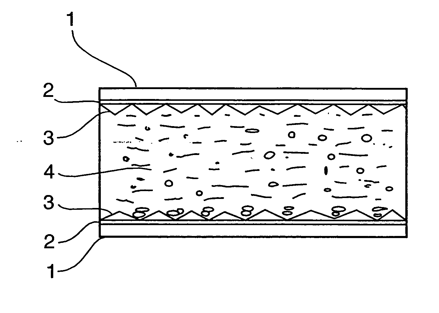
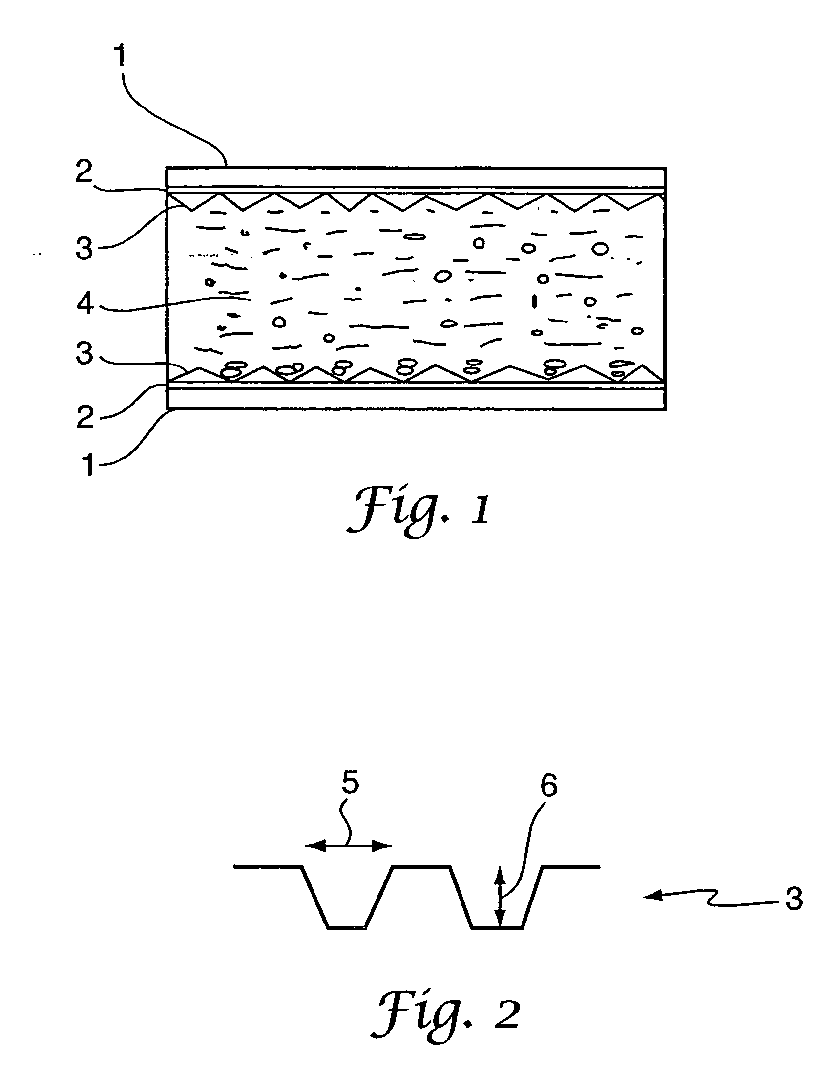
[0039] The display cell of FIG. 1 comprises opposed spaced-apart glass or plastic plate substrates 1, each provided with transparent electrode patterns 2 on its inner surface. Alignment grating layers 3 are provided on each inner surface, on top of the electrodes 2. The grating layers 3 have a pitch 5 and a depth 6. A layer of a nematic LC material 4 is sandwiched between the substrates 1, having dissolved in it a photocurable monomer. Curing of the monomer by shining UV light through only one of the substrates 1 causes a polymer coating to form on the alignment structure 2 on that substrate. The cell changes after polymerisation from a symmetrical cell to an unsymmetrical cell.

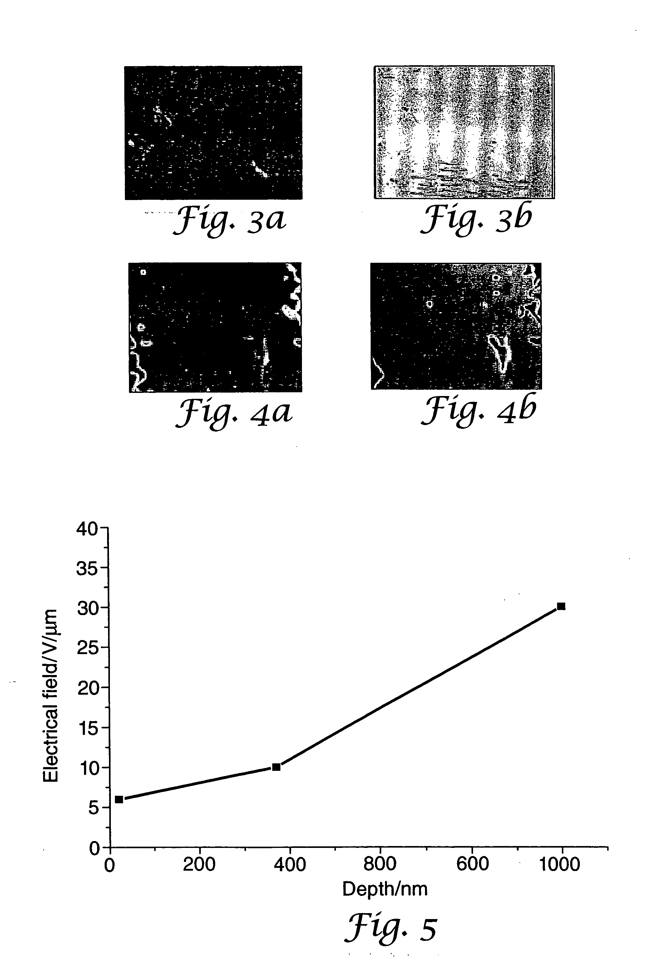
[0040] Experimentally we have used monogratings and post arrays with 200, 400 and 1000 nm depth. The thickness of the cells was varied between 2 to 5 μm using photocured glue with ball spacers on the boundary of the cell between the substrates. The cells were filled with a LC of positive dielectric anisotrop...


PUM

PropertyMeasurementUnit
glass transition temperatureaaaaaaaaaa
depthaaaaaaaaaa
grating depthaaaaaaaaaa

Abstract

A bistable liquid crystal device comprises first and second cell walls enclosing a layer of nematic liquid crystal material. Electrodes on at least one cell wall apply an electric field across at least some of the liquid crystal material. The inner surface of the cell wall includes a grating alignment structure having a polymeric material coating contacting the liquid crystal material and is substantially insoluble therein. Two stable molecular configurations can to exist in the nematic layer in response to suitable electrical signals applied to the electrodes.

Description

FIELD OF THE INVENTION [0001] This invention relates to bistable nematic liquid crystal devices and their manufacture. BACKGROUND OF THE INVENTION [0002] Pixel bistability is a desirable attribute for a liquid crystal display (“LCD”) because this eliminates the need constantly to refresh the display or to employ a silicon memory device behind each pixel, which becomes prohibitively expensive as the number of pixels increases. With bistability, only pixels that need to be changed need addressing, and simple matrix addressing may be employed. [0003] Bistable LCDs are known which employ chiral tilted smectic liquid crystals, for example chiral smectic C materials, which exhibit ferroelectricity. However, there are many problems with ferroelectric LCDs, including a paucity of stable, room-temperature materials, wide-temperature-range materials, and structural defects which result from mechanical stress. An attempt to reduce mechanical stress defects is described by V Vorflusev and S Kum...

Claims


Application Information

Patent Timeline
Patent Type & Authority Applications(United States)
IPC IPC(8): G02F1/1337G02F1/139
CPCG02F1/13378G02F2001/133765G02F1/1391G02F1/133765
Inventor SIKHARULIDZE, DAVID
Owner HEWLETT PACKARD DEV CO LP
Why Eureka
Try Eureka