Wavelength division multiplexer

a wavelength division multiplexer and wavelength division technology, applied in the field of wavelength division multiplexers, can solve the problems of large equipment size, high installation cost, large equipment size and high installation cost, and increase the cost, and achieve the effects of preventing characteristic deterioration, good wavelength division multiplexing characteristics, and small siz

Inactive Publication Date: 2005-05-05
MAXELL HLDG LTD
View PDF2 Cites 7 Cited by
  • Summary
  • Abstract
  • Description
  • Claims
  • Application Information

AI Technical Summary

Benefits of technology

[0012] In view of the foregoing, an object of the present invention is to prevent characteristic deterioration depending on a polarization surface when combining or separating light having more than two wavelengths with one optical component, and provide a multilayer filter and an optical component for wavelength division multiplexing which achieve good wavelength division multiplexing characteristics with a small size, allow flexible selection of bonding material used for bonding a plurality of substrates, and have good retaining characteristics while transmitting light.
[0013] Another object of the present invention is to prevent characteristic deterioration depending on a polarization surface when combining or separating light having more than two wavelength bands with one optical component, and provide a multilayer filter and an optical component for wavelength division multiplexing which achieves good wavelength division multiplexing characteristics with a small size.
[0023] The present invention allows providing a small-size and low-cost wavelength division multiplexer with good characteristics for combining or separating at least three-wavelength multiplexed light into three wavelength band light.

Problems solved by technology

It is, however, necessary to use a plurality of 3-terminal modules of at least one less than the number of wavelength bands, which requires high equipment costs, a large area, and high installation costs.
However, since a split angle of light is small, incorporation of a transmitting laser and a receiving diode requires a long optical path, which results in a large equipment size and high installation costs.
On the other hand, to reduce the equipment size, it is necessary to use a laser diode array, resulting in cost increase.
This, however, causes large divergence between P-wave and S-wave of outgoing light, deteriorating division multiplexer characteristics.
This results in wavelength shift and optical characteristics variation.
It is therefore necessary to make a structure that prevents the resin from coming to the surface, resulting in cost increase.

Method used


Image

  • Wavelength division multiplexer
  • Wavelength division multiplexer
  • Wavelength division multiplexer

Examples


embodiment 1

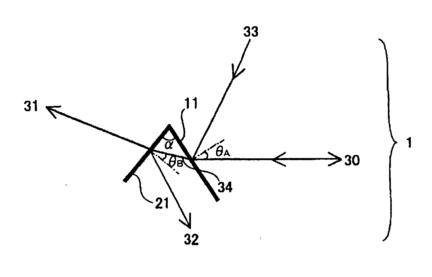
[0055]FIG. 1 is a schematic diagram illustrating an embodiment of a wavelength division multiplexer for separating wavelength multiplexed light consisting of at least three wavelength bands or combining wavelength bands into wavelength multiplexed light. In FIG. 1, an optical substrate and the like are omitted to schematically illustrate the wavelength division multiplexer.

[0056] As shown in FIG. 1, a wavelength division multiplexer 1 is composed of a first filter A 11 and a second filter B 21. The first filter A 11 and the second filter B 21 are supported by a single optical substrate or a plurality of optical substrates integrated together as described later, though not shown in this figure. Thus, the first filter A 11 and the second filter B 21 are configured to function as one optical element in a whole, thereby achieving miniaturization.

[0057] The light of λ3 moves from the direction indicated by a reference numeral 33. It is then reflected by the first filter A 11 in the dir...

embodiment 2

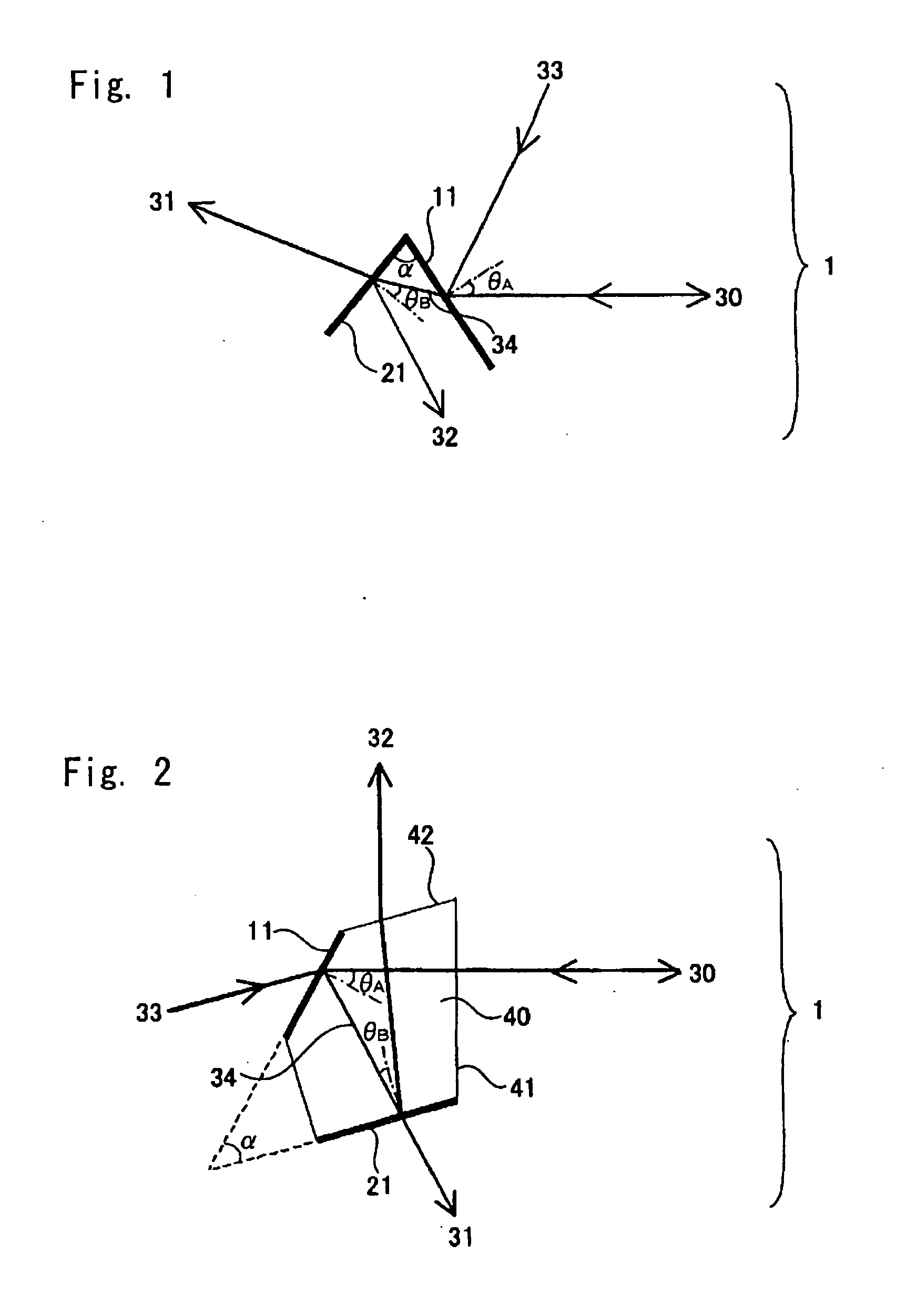
[0073]FIG. 2 is a schematic diagram illustrating another embodiment of a wavelength division multiplexer according to the present invention. The wavelength division multiplexer 1 shown in FIG. 2 is composed of the first filter A 11 and the second filter B 21 placed on different surfaces of a single substrate C 40. The single substrate may be replaced by a plurality of optical substrates integrated together.

[0074] As shown in FIG. 2, the light of λ3 coming from the direction 33 passes through the first filter A 11 and is combined with the light of λ1 and λ2 coming through the substrate, creating three-wavelength multiplexed light. On the other hand, two-wavelength multiplexed light of λ1 and λ2 is reflected by the first filter A 11 and enters the second filter B 21, where the two-wavelength multiplexed light is separated into the light of λ1 and the light of λ2.

[0075] A short wave pass filter is used for the first filter A 11, and an optical bandpass filter is used for the second f...

embodiment 3

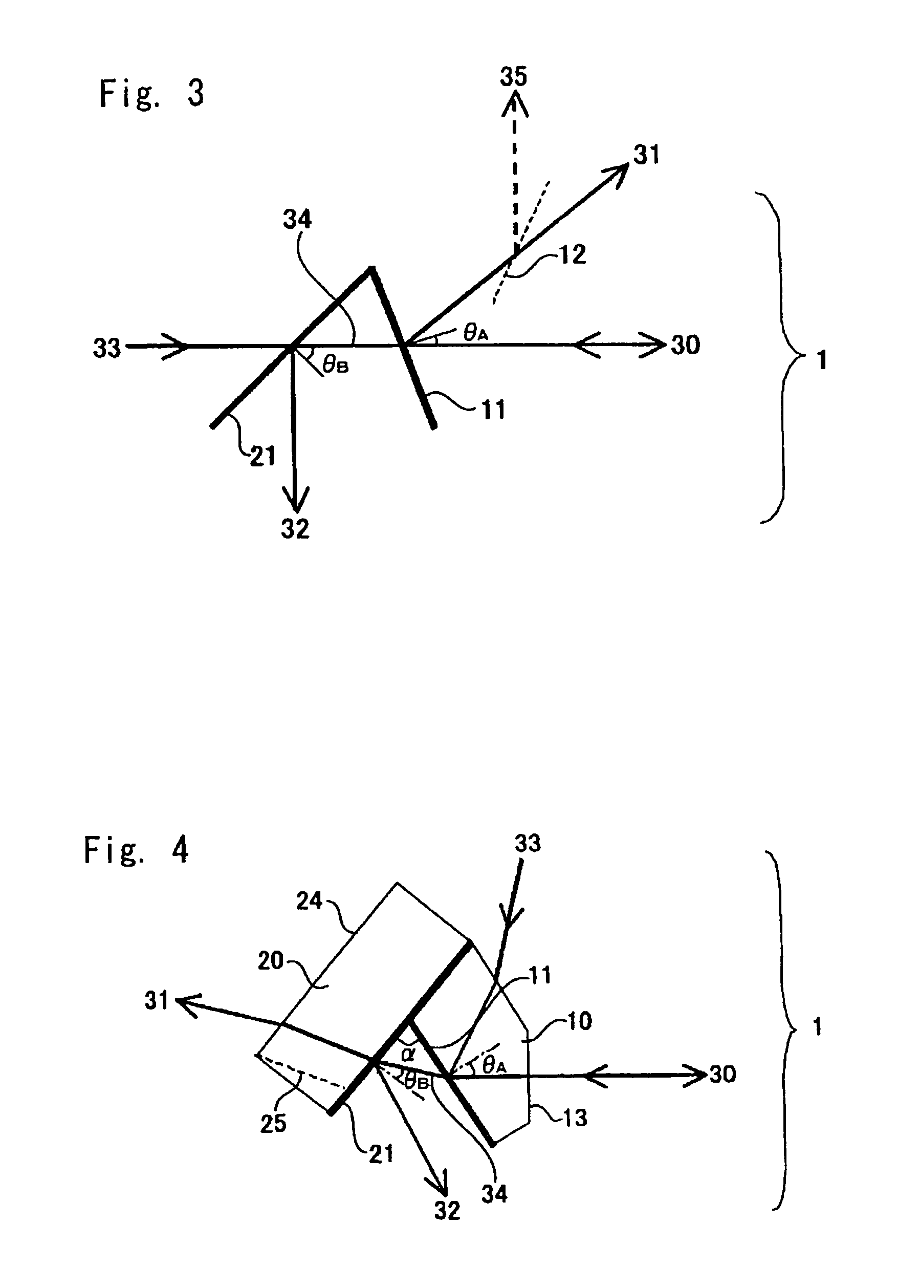
[0093]FIG. 3 is a schematic diagram illustrating yet another embodiment of a wavelength division multiplexer according to the present invention. The first filter A 11 combines or separates the light 31 of λ1 and the two-wavelength multiplexed light 34 of λ2 and λ3 into or from three-wavelength multiplexed light. The second filter B 21 combines or separates the light 32 of λ2 and the light 33 of λ3 into or from two-wavelength multiplexed light 34.

[0094] The relationship of the center wavelengths of the three-wavelength multiplexed light of this invention satisfies 0.94≦λ2 / λ1≦0.98 and 0.20≦λ3 / λ1≦0.94. This is because the present invention uses an edge filter to combine or separate wavelength multiplexed light, and it is difficult for the edge filter to separate the wavelength bands closer than the above range.

[0095] In the structure shown in FIG. 3 where the first filter A 11 combines or separates one wavelength band into or from three-wavelength multiplexed light, it is preferred t...


PUM


Abstract

The wavelength division multiplexer includes a single optical substrate or a plurality of optical substrates integrated together, on which the first optical filter and the second optical filter are placed. The center wavelengths of three wavelength bands, λ1, λ2, and λ3, satisfy: 0.92≦λ2 / λ1≦1.08, and 0.20≦λ3 / λ1≦0.92 or 1.08≦λ3 / λ1≦5.00. The first optical filter combines or separates light of λ3 and two-wavelength multiplexed light of λ1 and λ2. The second optical filter combines or separates light of λ1 and light of λ2.

Description

CROSS-REFERENCE TO RELATED APPLICATION [0001] The present invention is related to Japanese Patent Applications Serial No. 2003-336056, and 2003-404071, which are hereby incorporated. BACKGROUND OF THE INVENTION [0002] 1. Field of the Invention [0003] The present invention relates to a wavelength division multiplexer. [0004] 2. Description of Related Art [0005] A dielectric multilayer film is in wide use as an antireflection film coated on an eyeglass lens, a color separation filter for TV coated on a glass substrate, and so on. For example, the dielectric multilayer film is used for a color separation filter used in a liquid crystal projector, camera, and so on. It is also used for a laser detection mirror in a digital versatile disk (DVD) device and so on. When use for the laser detection mirror, the dielectric multilayer film is placed between two glass prism substrates so that light is incident on the dielectric multilayer film at a certain angle. [0006] In the field of communica...

Claims


Application Information

Patent Timeline
Patent Type & Authority Applications(United States)
IPC IPC(8): G02B27/14
CPCG02B27/145
Inventor MINAKAWA, YOSHIAKIMARO, TSUYOSHI
Owner MAXELL HLDG LTD
Why Eureka
Try Eureka