

Field emission-type electron source
a field emission and electron source technology, applied in the manufacture of electric discharge tubes/lamps, discharge tubes luminescnet screens, electrode systems, etc., can solve the problems of deterioration of electron emission efficiency, voltage to be adequately applied, and deterioration of electron emission characteristics
- Summary
- Abstract
- Description
- Claims
- Application Information
AI Technical Summary
Benefits of technology
Problems solved by technology
Method used
Image

Examples
Embodiment Construction
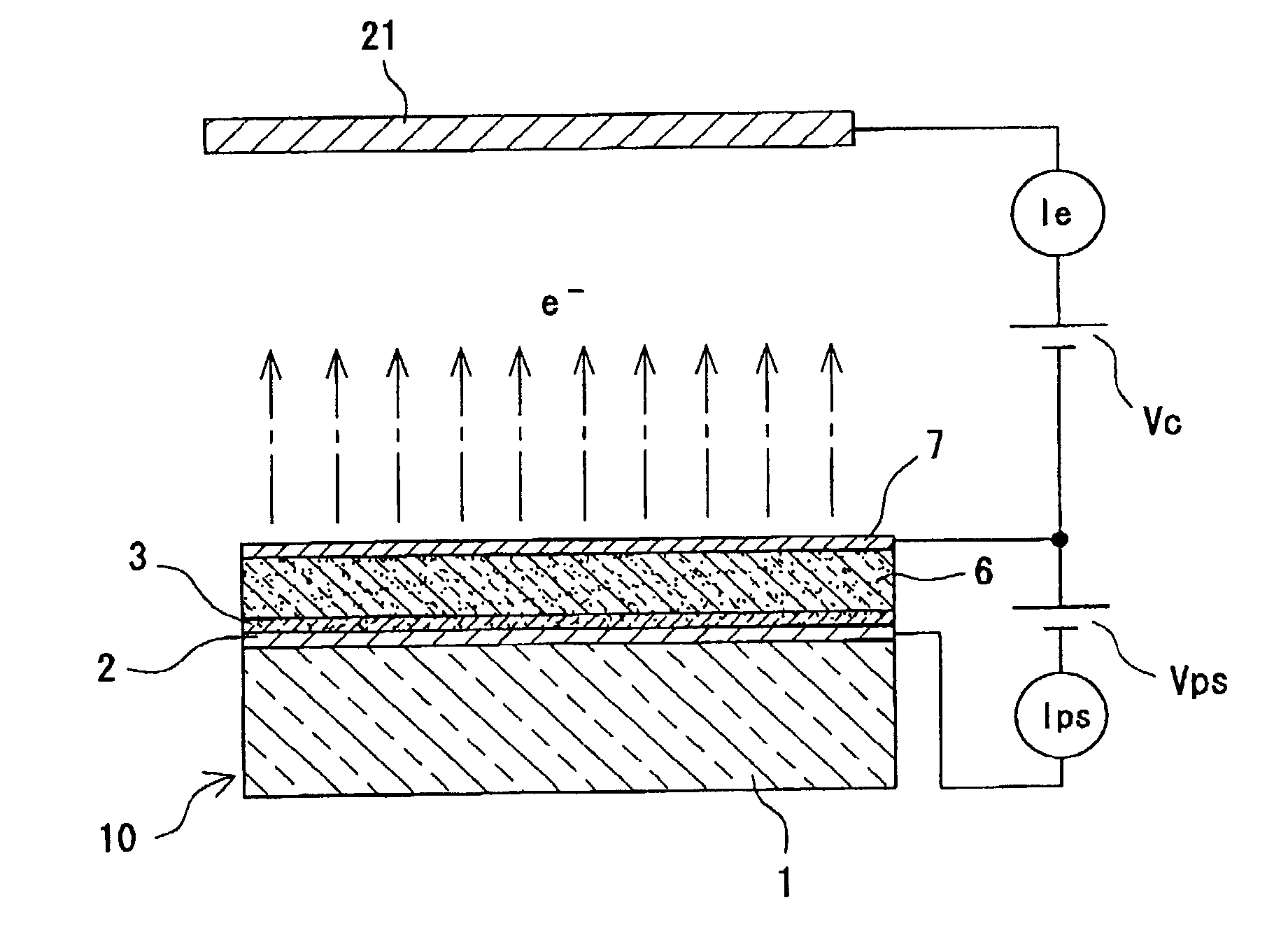
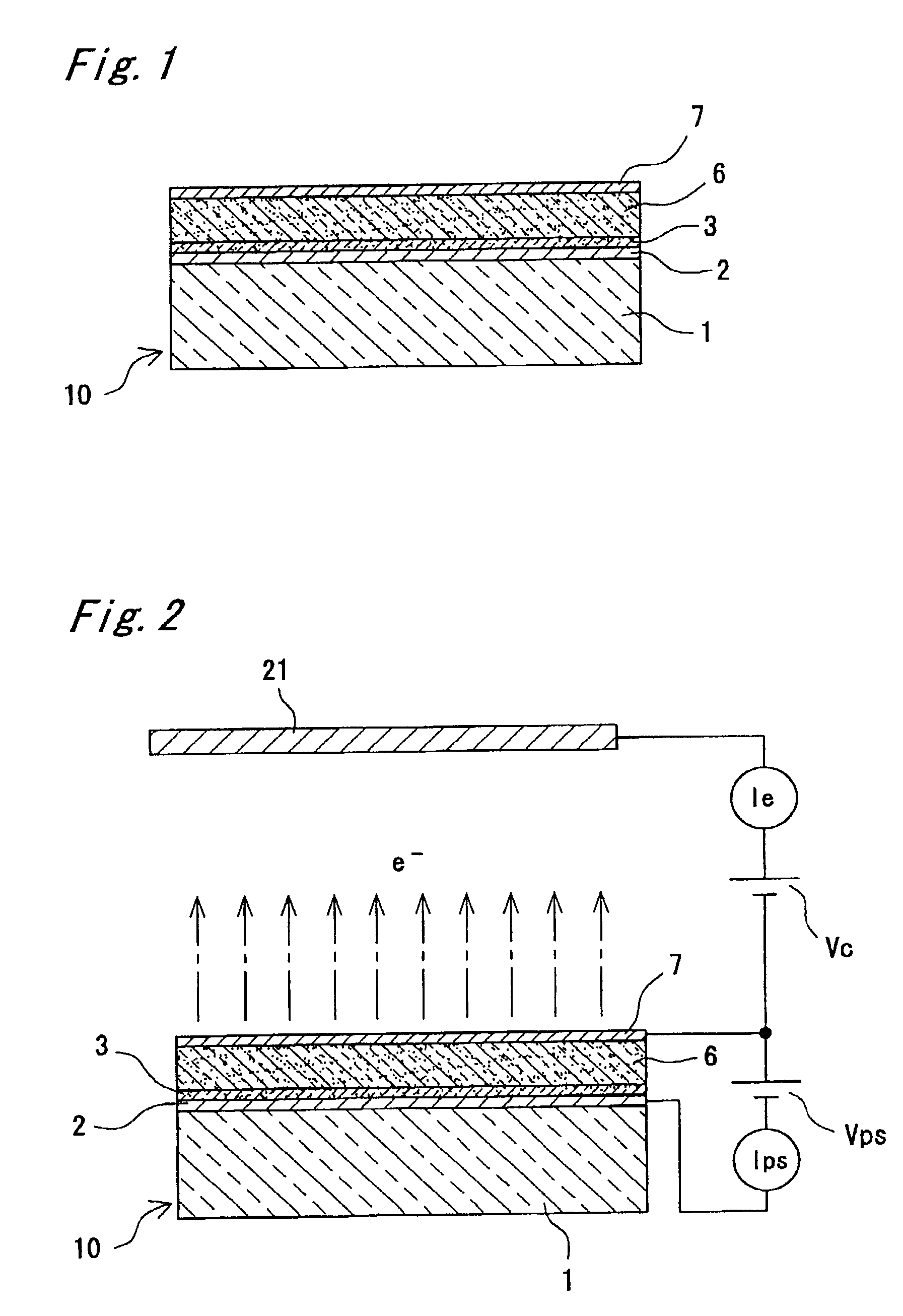
[0137] With reference to FIG. 11, a measurement result of electron emission characteristics in both states before and after an actually produced electron source 10 through the manufacturing process according to the fourth embodiment was subjected to a heat treatment will be described below.
[0138] In this example, a silicon substrate was used as the substrate 1, an n-type polycrystalline silicon layer being used as the lower electrode 2, an oxidized porous polycrystalline silicon layer being used as the electron transit layer 6 (strong field drift layer), a zirconium carbide layer being used as the conductive carbide layer 7e of the surface electrode 7, and a platinum layer being used as the noble metal layer 7f of the surface electrode 7. The thickness of the conductive carbide layer 7e was 2 nm, and the thickness of the noble metal layer 7f was 4 nm. The conductive carbide layer 7e was formed through an RF magnetron sputtering method using a target consisting of zirconium carbide u...
PUM
| Property | Measurement | Unit |
|---|---|---|
| thickness | aaaaa | aaaaa |
| thickness | aaaaa | aaaaa |
| thickness | aaaaa | aaaaa |
Abstract
Description
Claims
Application Information