Printed circuit board memory module with embedded passive components

a technology of passive components and printed circuit boards, applied in the field of printed circuit boards, can solve problems such as performance-affecting variances from nominal resistances, and achieve the effects of precise output signals, minimizing the surface area of pc boards, and minimizing the length of conductive paths

Inactive Publication Date: 2005-05-05
NETLIST INC
View PDF9 Cites 73 Cited by
  • Summary
  • Abstract
  • Description
  • Claims
  • Application Information

AI Technical Summary

Benefits of technology

[0008] Broadly, the present invention is a VLP memory module, comprising a plurality of memory components (e.g., DRAMs) mounted on a printed circuit (PC) board, and a plurality of passive components embedded within the PC board in locations that minimize the PC board surface area occupied by the passive components, while also minimizing the lengths of the conductive paths between the memory components and the passive components. In a specific preferred embodiment, the passive components are located directly underneath the memory components, and the conductive paths between the passive components and the memory components are provided by conductive vias between the terminals of the embedded components and the memory components mounted above them on the surface of the board. The passive components in the specific preferred embodiment are thick film resistors, either series damping resistors or differential damping resistors. By embedding the resistors directly beneath the memory components, there is enough space on the board to provide a set of termination resistors for each of the several memory components on the board, thereby eliminating the need for a single resistor to be shared by two or more memory components. The result is much “cleaner” and precise output signals; that is, the output signals are less noisy and suffer less variance from their nominal values.
[0009] Another aspect of the invention is that by embedding the passive components underneath the memory components, the passive components can be made larger than if they were to have their own dedicated board surface area. With resistors, in particular, their larger physical size (i.e., surface area) offers the advantage that absolute deviations from their nominal dimensions will result in much smaller deviations from their nominal resistance values. Specifically, the embedded thick film resistors are made with resistive inks that have fixed sheet resistance values. The resistive ink is printed between a pair of spaced-apart contact pads, thereby providing a resistor with a defined surface area and thus a defined resistance, the surface area and thus the resistance being within known and manageable tolerances. Typical embedded resistors may have tolerances of, for example, ±15% in their physical dimensions. Such wide tolerances may result in performance-affecting variances from their nominal resistances when the surface area of the resistor is relatively small. By substantially increasing the surface area of the resistor, however, the effect on the resistance value of such variations in the physical dimensions is proportionately reduced.
[0010] As will be further appreciated from the detailed description that follows, the advantages discussed above, as well as others that will be appreciated by those skilled in the pertinent arts, are provided in a PC board module that can be easily and economically manufactured with known circuit board manufacturing equipment and techniques.

Problems solved by technology

Such wide tolerances may result in performance-affecting variances from their nominal resistances when the surface area of the resistor is relatively small.

Method used


Image

  • Printed circuit board memory module with embedded passive components
  • Printed circuit board memory module with embedded passive components
  • Printed circuit board memory module with embedded passive components

Examples


Embodiment Construction

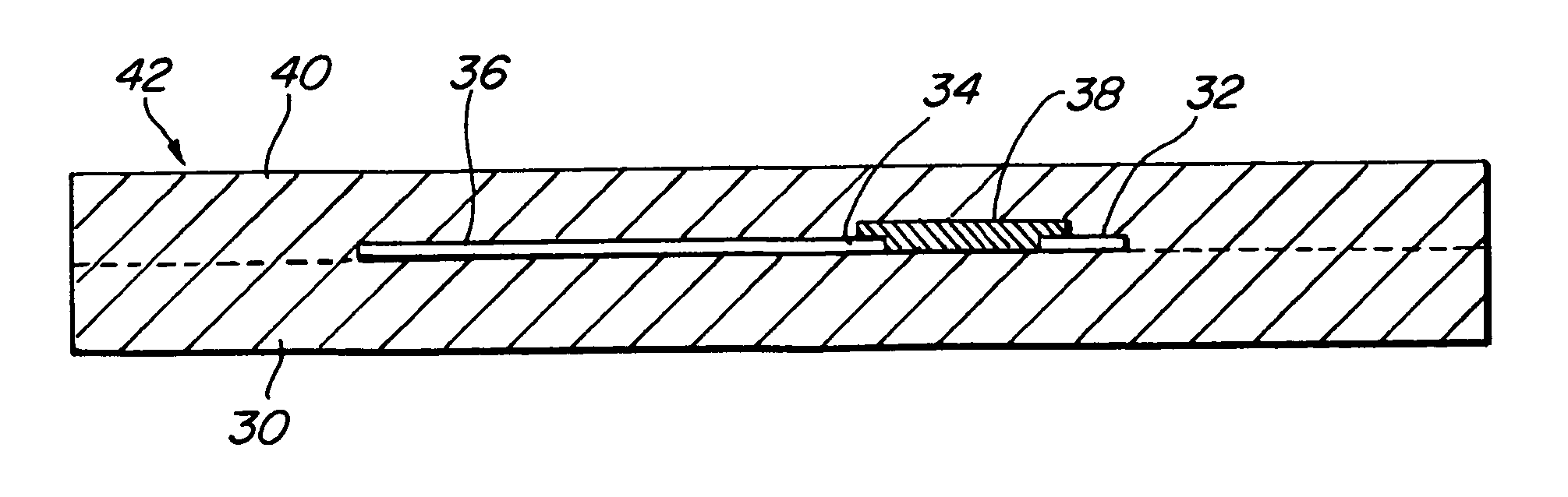
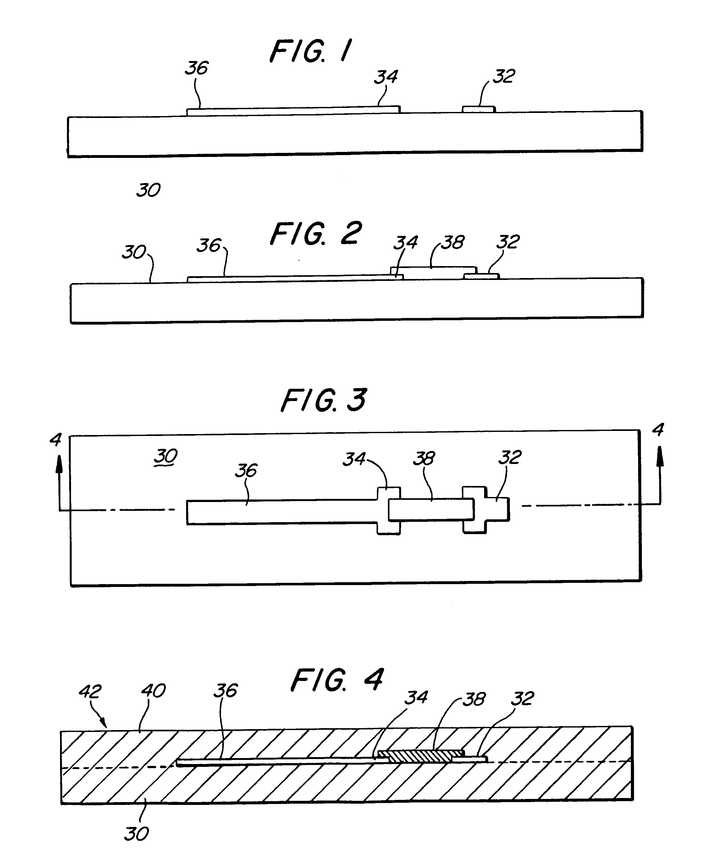
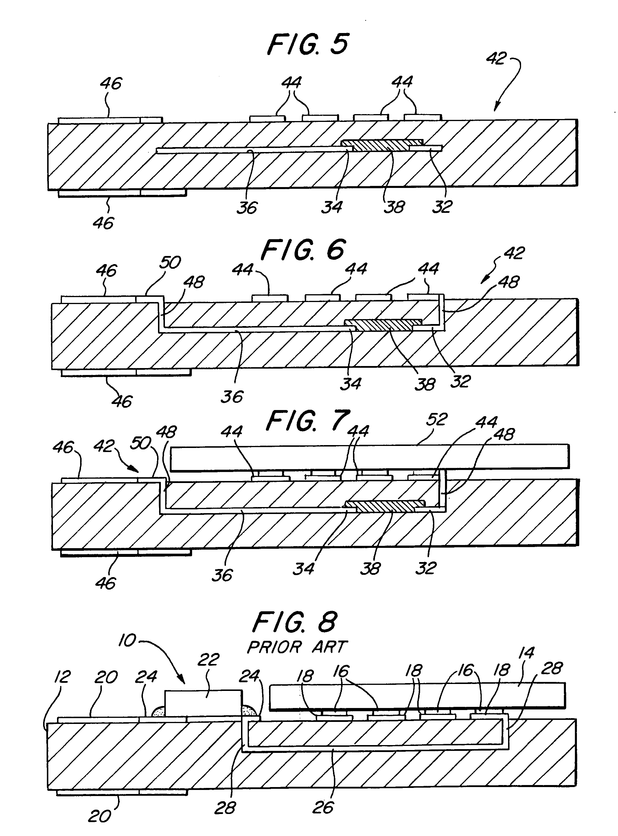
[0022] Referring first to FIG. 8, a typical, prior art PC board memory module 10 is shown. The module 10 comprises a printed circuit board 12 on which is mounted a plurality of solid state memory components 14, such as DRAMs, only one of which is shown. The DRAM 14 typically has short terminal contacts 16, which may be of the type known as a “ball grid array.” The DRAM terminal contacts 16, in turn, are soldered to conductive contact pads 18 formed on the surface of the board 12 by conventional means, well-known in the art. One edge of the board 12 is provided with a plurality of connector contacts 20, which allow the board 12 to be plugged into a mating socket (not shown) on a larger board or “motherboard” (not shown).

[0023] Passive components, such as a termination resistor 22, are mounted on the surface of the board 12 between the DRAM 14 and the connector contacts 20. The termination resistor 22 is a typical “surface mount technology” (SMT) component, which is soldered to condu...


PUM


Abstract

A memory module includes a plurality of memory components mounted on a printed circuit board, and a plurality of passive components embedded within the board directly underneath the memory components to minimize the space occupied by the passive components and the lengths of the required conductive traces. The passive components and the memory components are connected by conductor-filled vias between the contacts of the embedded components and the memory components mounted above them on the board surface. The passive components may be thick film resistors, either series damping resistors or differential damping resistors. By embedding the resistors directly beneath the memory components, there is enough space on the board to provide a set of termination resistors for each of the several memory components on the board, thereby eliminating the need for a single resistor to be shared by two or more memory components, resulting in more precise output signals.

Description

CROSS-REFERENCE TO RELATED APPLICATIONS [0001] This application claims the benefit, under 35 U.S.C. § 119(e), of co-pending provisional application No. 60 / 516,684; filed Nov. 3, 2003, and of co-pending provisional application No. 60 / 553,113; filed Mar. 15, 2004, the disclosures of which are incorporated herein by reference.FEDERALLY SPONSORED RESEARCH OR DEVELOPMENT [0002] Not Applicable BACKGROUND OF THE INVENTION [0003] The present invention relates broadly to the field of printed circuits, and more particularly to a printed circuit boards on which are mounted solid state memory components. More specifically, the present invention relates to a “very low profile” (VLP) memory module, comprising a plurality of solid state memory components on a circuit board that also includes discrete surface mount (“SMT”) passive components, or thick film resistors that are embedded within the circuit board material. [0004] Modern computer systems typically employ one or more memory modules, each ...

Claims


Application Information

Patent Timeline
Patent Type & Authority Applications(United States)
IPC IPC(8): G11C5/00H05K1/00H05K1/02H05K1/16
CPCH05K1/023H05K1/0237H05K1/0246H05K2201/10159H05K1/167H05K2201/09236H05K1/0298
Inventor GERVASI, WILLIAM M.BHAKTA, JAYESH R.PAULEY, ROBERT S.
Owner NETLIST INC
Why Eureka
Try Eureka