

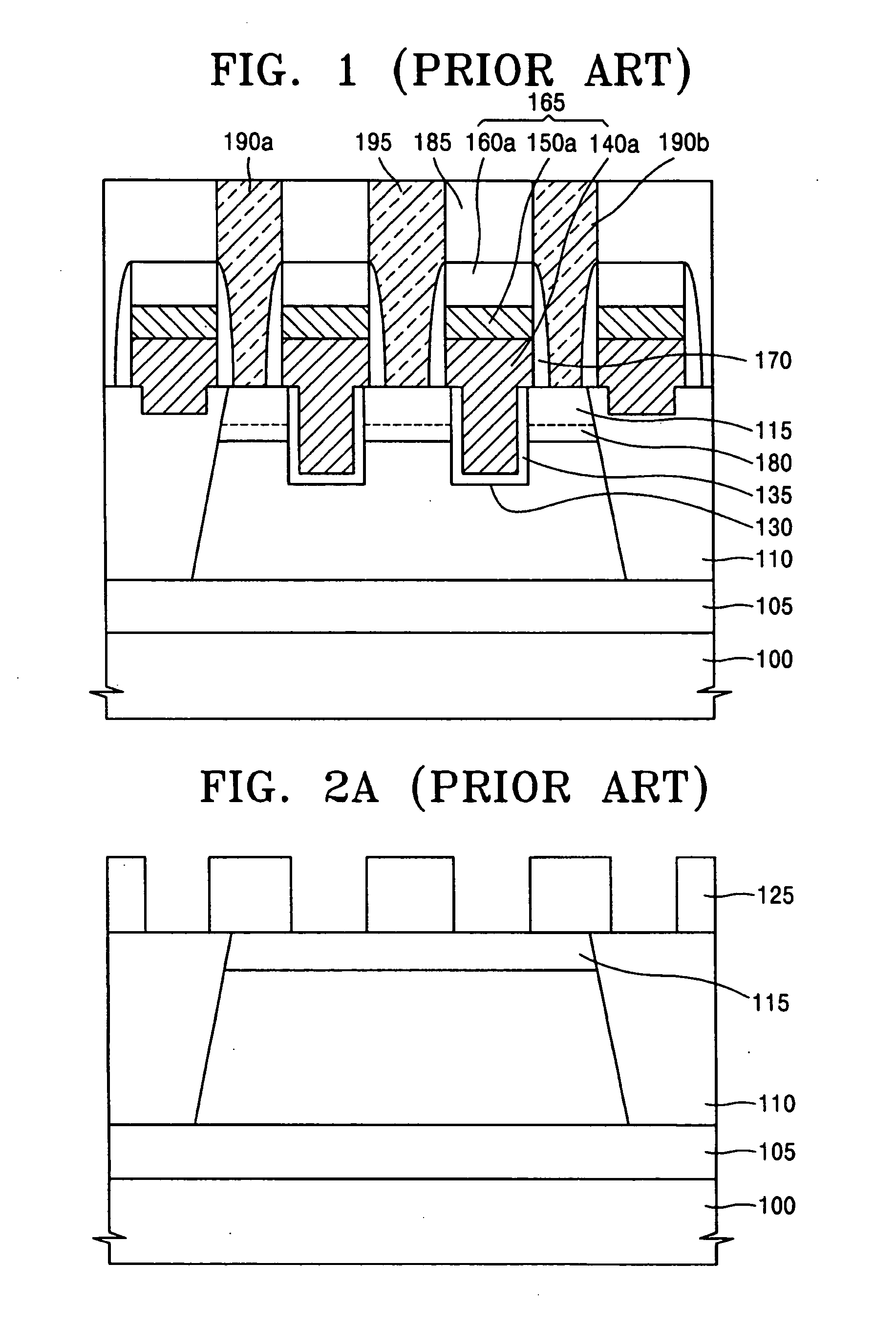
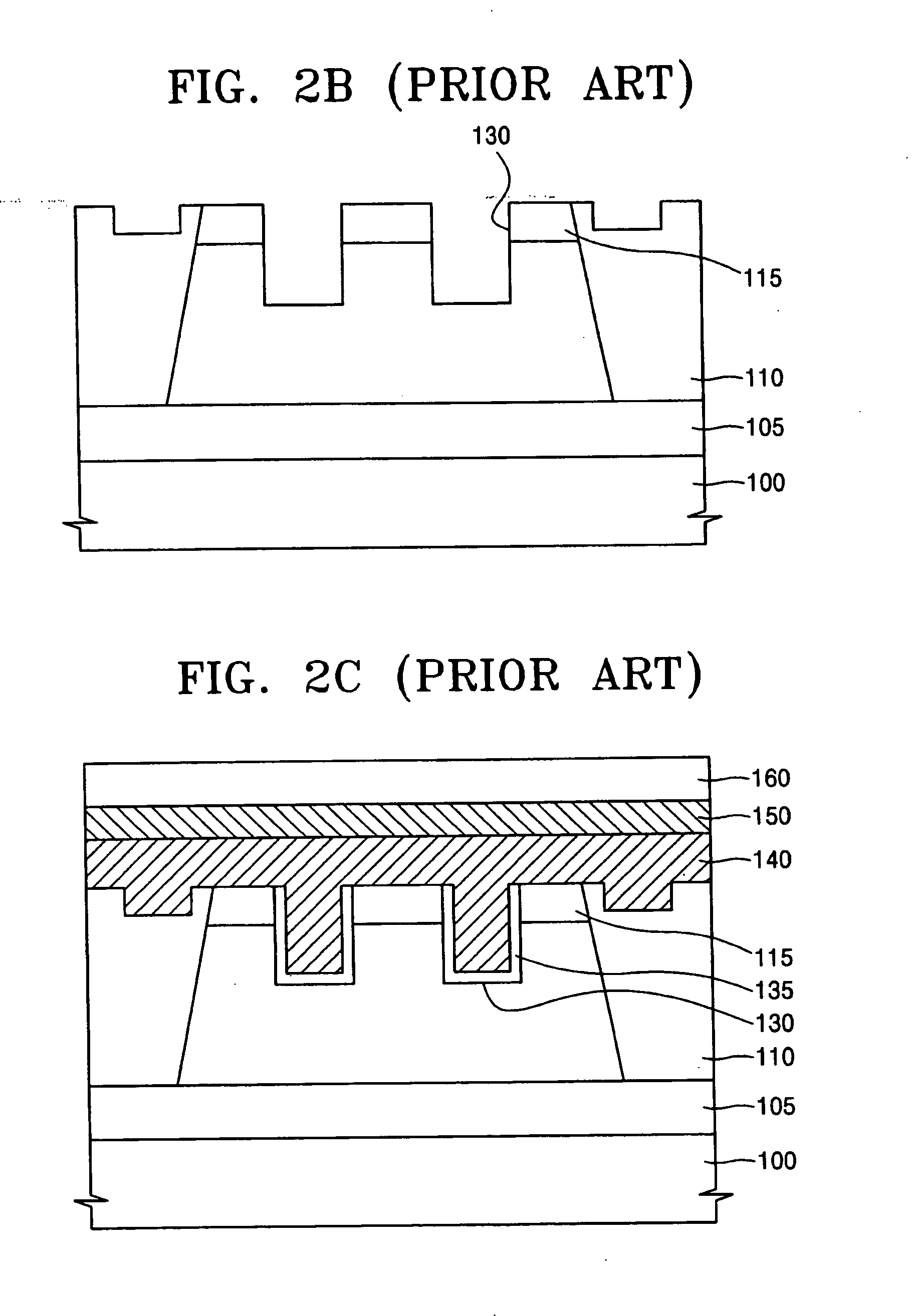
Method of fabricating recess channel array transistor
- Summary
- Abstract
- Description
- Claims
- Application Information
AI Technical Summary
Benefits of technology
Problems solved by technology
Method used
Image

Examples
Embodiment Construction
[0041] The present invention will now be described more fully with reference to the accompanying drawings, in which exemplary embodiments of the invention are shown. The invention may, however, be embodied in many different forms and should not be construed as being limited to the embodiments set forth herein; rather, these embodiments are provided so that this disclosure will be thorough and complete, and will fully convey the concept of the invention to those skilled in the art.
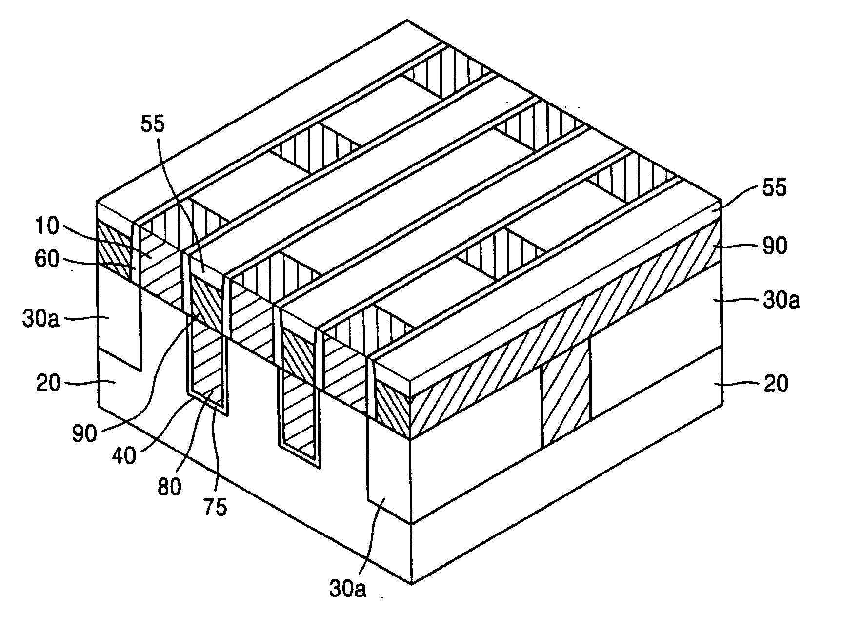
[0042]FIGS. 3 through 13 are perspective views illustrating a method of fabricating a recess channel array transistor according to one embodiment of the present invention.
[0043] Referring to FIG. 3, a semiconductor substrate 20 is ion-implanted to form a necessary impurity region (not shown). Then, a polysilicon layer 10 is formed on the semiconductor substrate 20. The impurity regions formed using ion implantation into the semiconductor substrate 20 includes source / drain impurity regions. For example, wh...
PUM
 Abstract
Description
Claims
Application Information