Tensile Contact Etch Stop Layer (CESL) For Radio Frequency (RF) Silicon-On-Insulator (SOI) Switch Technology

Inactive Publication Date: 2018-03-08
NEWPORT FAB
View PDF5 Cites 0 Cited by
  • Summary
  • Abstract
  • Description
  • Claims
  • Application Information

AI Technical Summary

Benefits of technology

[0010]In one embodiment, the CESL is formed over both re-channel SOI CMOS transistors (including the RF switch transistors) and p-channel SOI CMOS transistors fabricated on the same substrate. Because the same CESL structure is formed over both the n-channel and p-channel transistors, the fabrication process is simplified. While the on-resistances of the n-channel SOI CMOS transistors are reduced (thereby advantageously reducing the on-resistance RON of the RF switch), the on-resistances of the p-channel SOI CMOS transistors are increased. However, because the p-channel transistors are only used in non-critical logic or analog circuitry in the RF switch application, the increase in the on-resistances of the p-channel transistors is acceptable.
[0011]Another embodiment includes methods for fabricating the SOI CMOS transistor of the present invention. One method includes forming a plurality of SOI CMOS transistors, including a plurality of series-connected transistors of an RF switch, on a thi

Problems solved by technology

However, traditional CMOS scaling is not an acceptable path for on-resistance reduction in this application, because such scaling would prevent the resulting transistors from meeting the required operating voltages and power handling requirements.
That is, while transistors having channel lengths of less than about 0.13 microns would advantageously exhibit low on-resistances, such transistors would not be able to handle the operating voltages (or power requirements) associated with an RF switch application.
Moreover, it would not be cost effective to use SOI CMOS tran

Method used


Image

  • Tensile Contact Etch Stop Layer (CESL) For Radio Frequency (RF) Silicon-On-Insulator (SOI) Switch Technology
  • Tensile Contact Etch Stop Layer (CESL) For Radio Frequency (RF) Silicon-On-Insulator (SOI) Switch Technology
  • Tensile Contact Etch Stop Layer (CESL) For Radio Frequency (RF) Silicon-On-Insulator (SOI) Switch Technology

Examples


Embodiment Construction

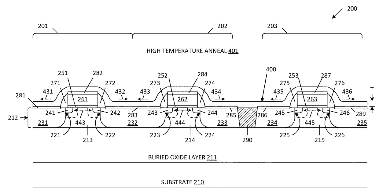
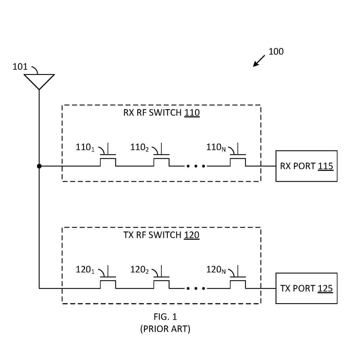
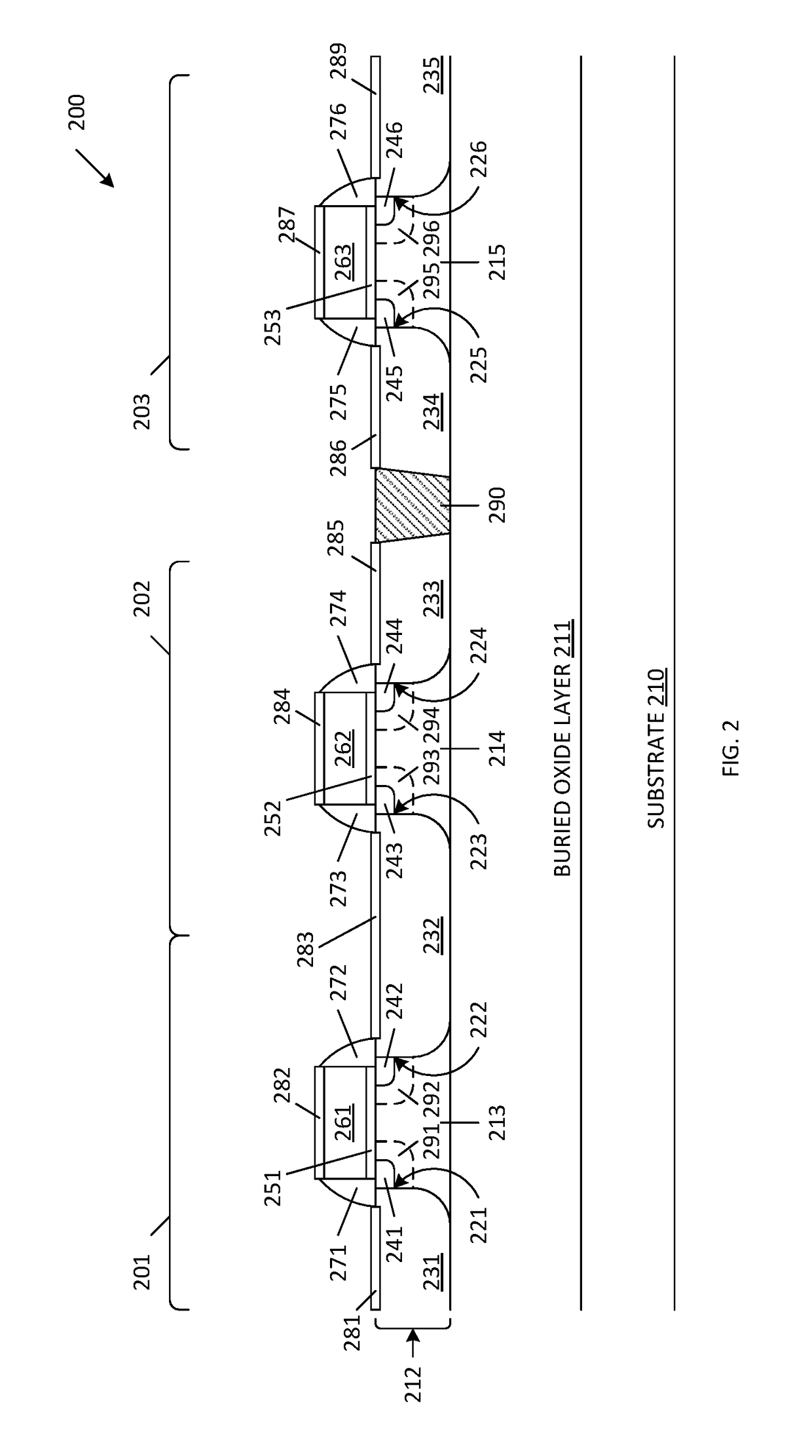
[0017]FIG. 2 is a cross-sectional view of an SOI CMOS structure 200, which includes n-channel SOI CMOS transistors 201-202 and p-channel SOI CMOS transistor 203. In accordance with one embodiment, transistors 201-202 may represent series-connected transistors of an RF switch. For example, transistors such as transistors 201-202 may be used to replace the series-connected transistors 1101-110N of the receiver RF switch 110 (and the series-connected transistors 1201-120N of the transmitter RF switch 120) in one embodiment of the present invention. In this embodiment, transistors having the construction of transistors 201-203 are also used to implement non-critical logic and analog circuitry that supports these RF switches (e.g., logic and circuitry in the RF receiver port 115 and the RF transmit port 125). SOI CMOS transistors 201-203 are fabricated on a thin silicon layer 212, which is located on a buried insulator layer 211 (e.g., silicon oxide), which in turn, is located on a subst...


PUM


Abstract

A radio frequency switch includes a plurality of n-channel SOI CMOS transistors connected in series, wherein each of these transistors has a gate width of at least about 0.13 microns. A contact etch stop layer (CESL) structure having a relatively large thickness of at least about 1000 Angstroms is formed on silicide regions of the n-channel SOI CMOS transistors, wherein the CESL structure places a tensile stress on channel regions of the n-channel SOI CMOS transistors, thereby reducing the on-resistances of the n-channel SOI CMOS transistors. The CESL structure is also formed over p-channel SOI CMOS transistors fabricated on the same substrate as the n-channel SOI CMOS transistors. While the CESL structure also places a tensile stress on channel regions of the p-channel SOI CMOS transistors (increasing the on-resistances of these transistors), the on-resistances of the p-channel SOI CMOS transistors are non-critical in the RF switch application.

Description

FIELD OF THE INVENTION[0001]The present invention relates to the use of a contact etch stop layer (CESL) to introduce tensile stress to the channel regions of silicon-on-insulator (SOI) CMOS transistors used in high power applications such as radio frequency (RF) switching.RELATED ART[0002]FIG. 1 is a circuit diagram of a conventional radio frequency (RF) circuit 100, including an antenna 101, an RF receiver switch 110, an RF receiver port 115, an RF transmitter switch 120 and an RF transmitter port 125. RF receiver switch 110 includes a plurality of high-voltage field effect transistors (FETs) 1101-110N, which are connected in series (in a stack). The stack of high voltage FETs 1101-110N is controlled to route RF signals from antenna 101 to receive port 115. Similarly, RF transmitter switch 120 includes a stack of high-voltage FETs 1201-120N, which are controlled to route RF signals from transmit port 125 to antenna 101. As used herein, an RF signal is defined as a signal having a ...

Claims


Application Information

Patent Timeline
IPC IPC(8): H01L27/13H01L29/78H01L29/45H01L21/02H01L21/322
CPCH01L27/13H01L29/7843H01L29/458H01L21/0217H01L29/78696H01L21/3226H01L21/02274H01L21/02211H01L29/78621H01L21/02359H01L27/1203H01L29/665H01L29/6659H01L21/02318H01L27/092H01L21/84H01L21/823807H01L29/78606H01L29/7833
Inventor HURWITZ, PAUL D.
Owner NEWPORT FAB
Why Eureka
Try Eureka