
Method and system for power management in a gigabit Ethernet chip

a technology of gigabit ethernet and power management, applied in power management, high-level techniques, instruments, etc., can solve problems such as the limitation of non-native applications' use of hardware specific driver blocks b>110/b>, and the rise of new challenges

Inactive Publication Date: 2005-05-05
AVAGO TECH WIRELESS IP SINGAPORE PTE
View PDF2 Cites 116 Cited by
  • Summary
  • Abstract
  • Description
  • Claims
  • Application Information

AI Technical Summary

Benefits of technology

[0022] Certain aspects of the invention may be found in a method and system for managing power in a single chip device. Aspects of the method for managing power in a single chip device may comprise, determining internally from within the single chip device while in a communicating state, whether a power management status is set and/or whether a first power management event is received. If the power management status is set, a trans

Problems solved by technology

The proliferation of physical layer devices designed to meet the needs of high speed communication applications will, without a doubt, give rise to new challenges.
One challenge pertains to the development of high speed communications devices having optimized power consumption.
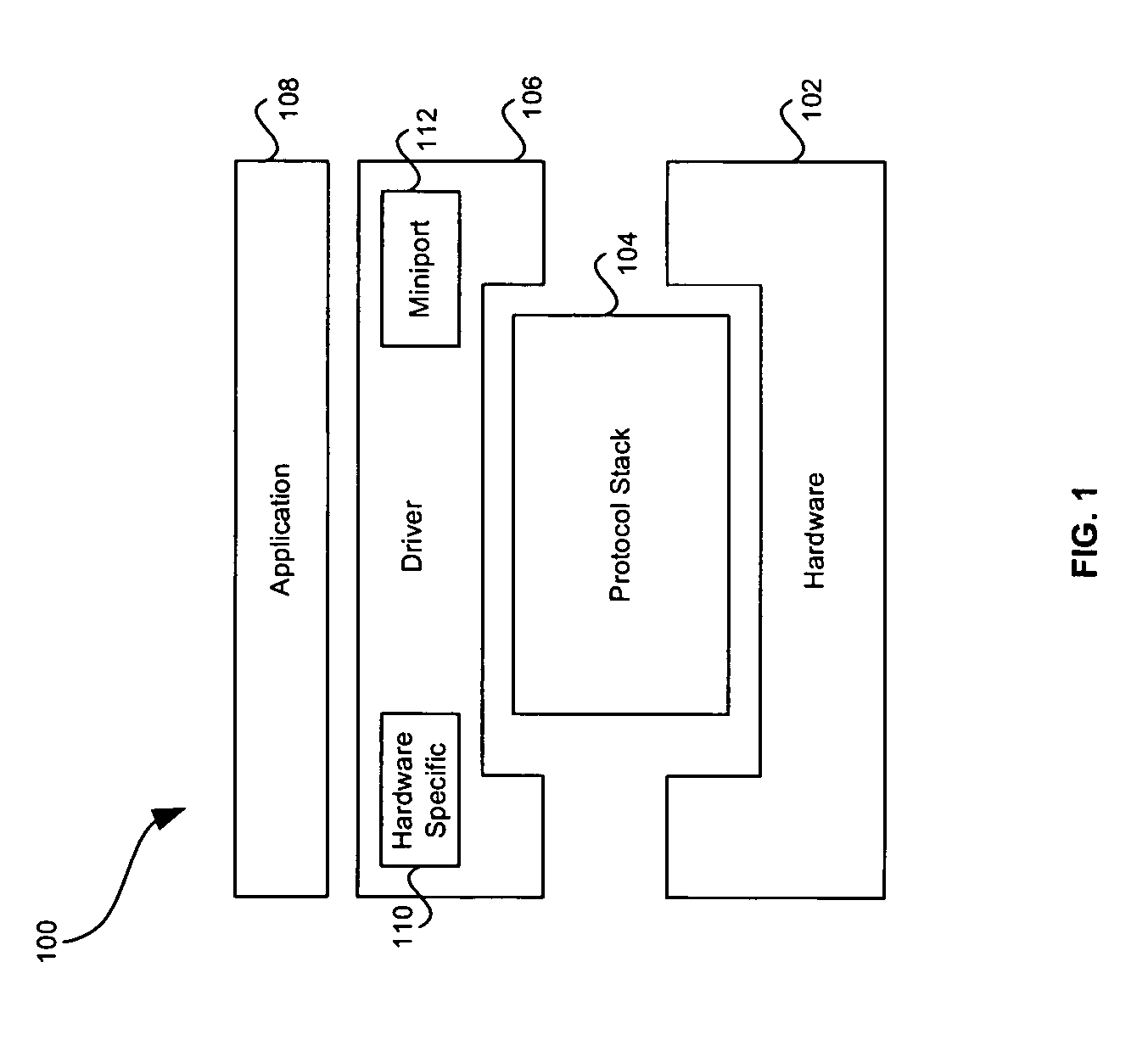
In this regard, the use of the hardware specific driver block 110 by non-native applications may be limited and in some instances, some non-native applications may not have the capability to interface with the hardware specific driver block 110.
Such an implementation may add excessive cost to the hardware required for the network interface controller and / or card (NIC), since additional memory and / or buffers may be required.
Furthermore, since additional software programming is required to control the functionality of the network interface card, the programming overhead may further increase the cost associated with the network interface card.
Moreover, in Gigabit Ethernet (GbE) wire-speed applications, these associated costs can obviously be prohibitively high.

Method used


Image

  • Method and system for power management in a gigabit Ethernet chip
  • Method and system for power management in a gigabit Ethernet chip
  • Method and system for power management in a gigabit Ethernet chip

Examples


Embodiment Construction

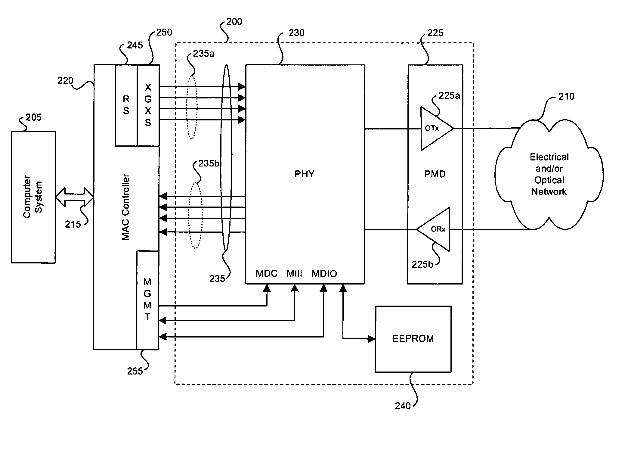
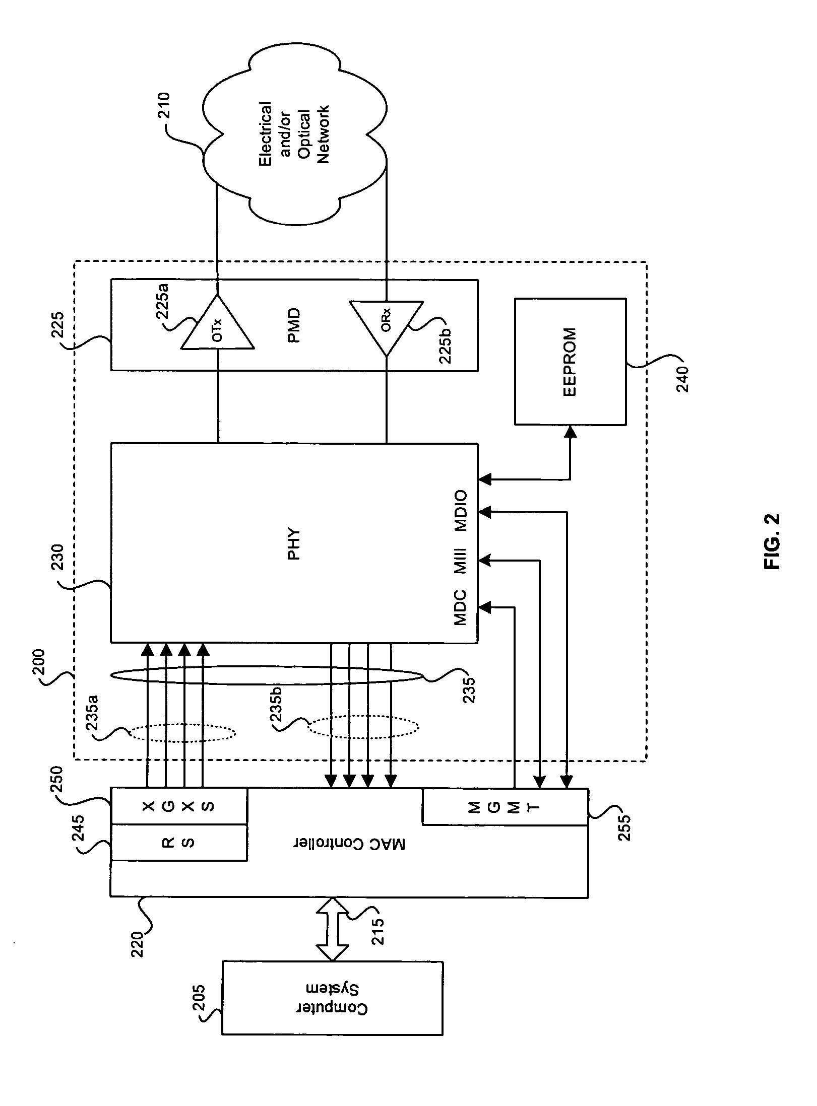
[0035] Aspects of the present invention relate to providing power management in an Ethernet controller chip. In particular, certain embodiments relate to a single chip device for a LAN on motherboard (LOM) and / or a network Interface Card (NIC) applications that may contain, for example, an integrated 10 / 100 / 1000BaseT transceiver and an on-chip power circuit controller and wake-on LAN (WOL) power switching circuit. The 10 / 100 / 1000BaseT transceiver may be referred to as a gigabit transceiver and may comprise a gigabit physical (PHY) layer device or a gigabit PHY (GPHY). The single chip device may also be adapted to support a plurality of legacy power management modes and may comprise a gigabit Ethernet (GbE) peripheral component interconnect (PCI) controller / interface, PCI-X, or peripheral component interconnect Express controller / interface, for example.

[0036] U.S. patent application Ser. No. 10 / 340,408 (Attorney Docket No. 13910US02) discloses an exemplary gigabit PHY that may be ut...


PUM


Abstract

Aspects of the invention for managing power in a single chip device may comprise, an internal finite state machine that, while in a communicating state, determines from within the single chip device whether a power management status is set and / or whether a first power management event is received. If the power management status is set, the finite state machine may transition from the communicating state to a power management event sent state. If the first power management event is received, the finite state machine may transition from the communicating state to a non-communicating state. The first power management event may be a turn off power management event. Furthermore, in instances where the power management status is set, it may be cleared, thereby causing the finite state machine to transition back to the communicating state. One or more power management control registers may be utilized for indicating power management status.

Description

CROSS-REFERENCE TO RELATED APPLICATIONS / INCORPORATION BY REFERENCE [0001] This application is a continuation-in-part of U.S. application Ser. No. 10 / 629,207 (Attorney Docket No. 13935US02) filed on Jul. 29, 2003. [0002] This application also make reference to, claims priority to and claims the benefit of U.S. Provisional Application Ser. No. 60 / 502,437 (Attorney Docket No. 15194US01) filed on Sep. 12, 2003. [0003] This application also make reference to: [0004] U.S. application Ser. No. ______ (Attorney Docket No. 13946US02) filed on Jul. 8, 2004; and [0005] U.S. application Ser. No. 10 / 353,440 (Attorney Docket No. 13948US02) filed on Jan. 29, 2003. [0006] The above stated applications are all incorporated herein by reference in their entirety.FIELD OF THE INVENTION [0007] Certain embodiments of the invention relate to power management. More specifically, certain embodiments of the invention relate to a method and system for power management in a gigabit Ethernet chip. BACKGROUND OF...

Claims


Application Information

Patent Timeline
IPC IPC(8): G06F1/32H04L12/12H04W52/02
CPCG06F1/3203G06F1/3209Y02B60/35H04L12/12Y02B60/34G06F1/3215Y02D30/50
Inventor HWANG, ANDREW S.
Owner AVAGO TECH WIRELESS IP SINGAPORE PTE
Learn More