Semiconductor integrated circuit

a technology of integrated circuits and semiconductors, applied in the direction of electronic circuit testing, measurement devices, instruments, etc., can solve the problem of difficult handling of memory b>50/b>

Inactive Publication Date: 2005-05-05
KK TOSHIBA
View PDF8 Cites 29 Cited by
  • Summary
  • Abstract
  • Description
  • Claims
  • Application Information

AI Technical Summary

Problems solved by technology

Accordingly, the memory 50 is difficul

Method used


Image

  • Semiconductor integrated circuit
  • Semiconductor integrated circuit
  • Semiconductor integrated circuit

Examples


first embodiment

(First Embodiment)

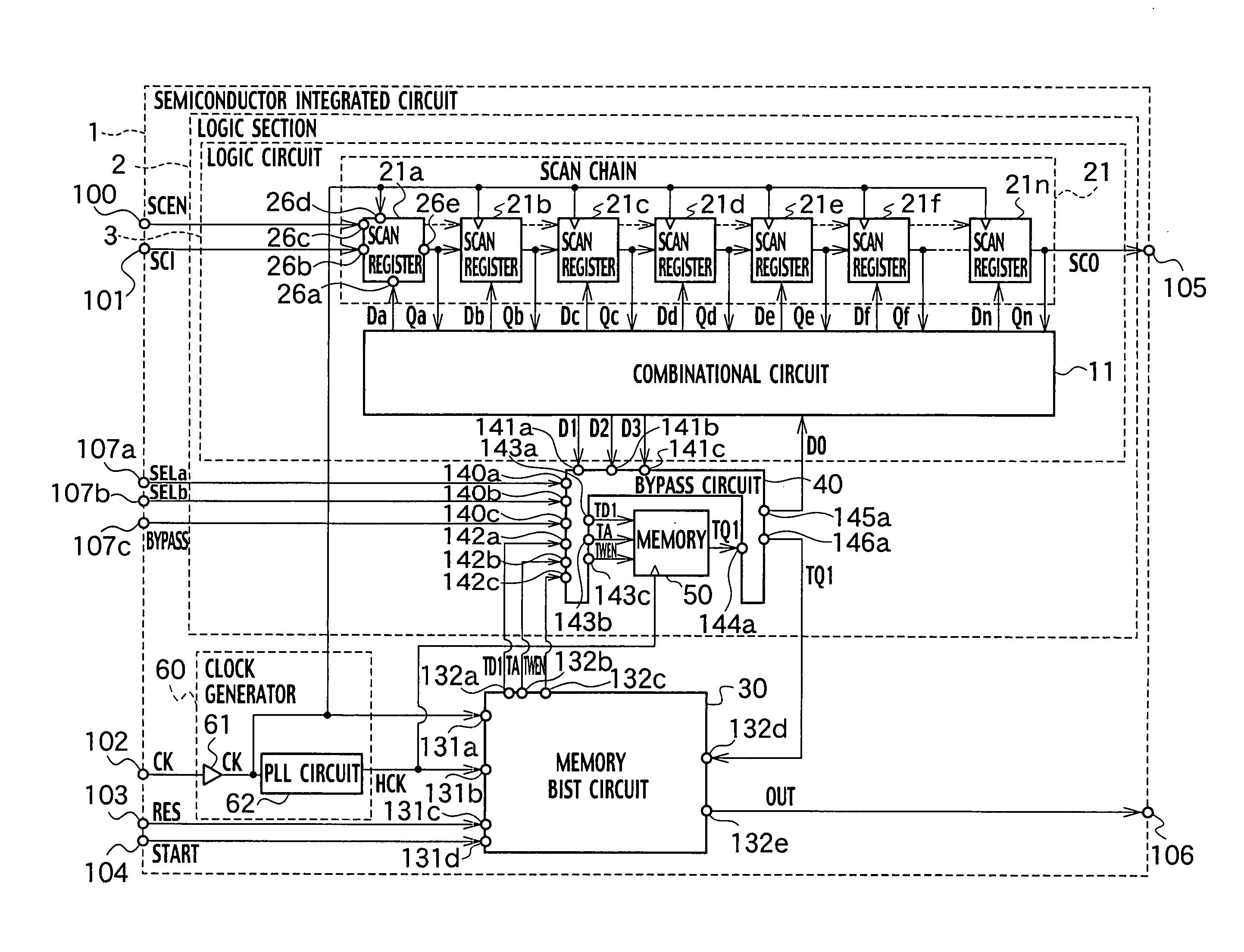
[0026] As shown in FIG. 1, a semiconductor integrated circuit 1 according to a first embodiment of the present invention includes a logic circuit 3 to be tested, a memory 50 connected the logic circuit 3 to be tested, a BIST circuit (memory BIST circuit) 30 for testing the memory 50, and a bypass circuit 40 connected between the memory 50 and the logic circuit 3 and between the memory 50 and the BIST circuit 30. The bypass circuit 40 has a parallel test path for testing the logic circuit 3 and the memory 50 in parallel, and a signal line test path for testing non-tested signal lines in the parallel test path, and the bypass circuit selectively switches the parallel test path and the signal line test path.

[0027] The memory 50, the bypass circuit 40 and the logic circuit 3 are included in a logic section 2. A clock generation circuit 60 is connected with the memory 50, the logic section 2 and the BIST circuit 30. The clock generation circuit 60 includes a buffer 61 ...

second embodiment

(Second Embodiment)

[0093] As shown in FIG. 11, a semiconductor integrated circuit 1b according to a second embodiment of the present invention includes a clock generator 60b, a logic BIST circuit 80 connected with the clock generator 60b, a logic section 2b connected with the clock generator 60b and the logic BIST circuit 80, and a BIST circuit (memory BIST circuit) 30b connected with the clock generator 60b, the logic BIST circuit 80 and the logic section 2b.

[0094] The clock generator 60b includes a buffer 61 connected with an external clock input terminal 102 and a PLL circuit 62 connected with the buffer 61. The buffer 61 buffers the external clock CK. The PLL circuit 62 multiplies frequency of the external clock CK, and generates a high-speed clock HCK.

[0095] For example, a so-called circuit “STUMPS (Self-Testing Using MISR and Parallel SRSGs)” can be used as the logic BIST circuit 80. The logic BIST circuit 80 includes an input terminal 181 connected with a logic test start s...


PUM


Abstract

A semiconductor integrated circuit includes: a logic circuit to be tested; a memory connected the logic circuit to be tested; a BIST circuit for testing the memory; and a bypass circuit connected between the memory and the logic circuit and between the memory and the BIST circuit, the bypass circuit has a parallel test path for testing the logic circuit and the memory in parallel, and a signal line test path for testing non-tested signal lines in the parallel test path, and the bypass circuit selectively switches the parallel test path and the signal line test path.

Description

CROSS REFERENCE TO RELATED APPLICATIONS [0001] This application is based upon and claims the benefit of priority from the prior Japanese Patent Applications No. P2003-370947, filed on Oct. 30, 2003; the entire contents of which are incorporated herein by reference. BACKGROUND OF THE INVENTION [0002] 1. Field of the Invention [0003] The present invention relates to a semiconductor integrated circuit, and, more particularly, relates to a semiconductor integrated circuit including a Buit-In Self Test (BIST) circuit. [0004] 2. Description of the Related Art [0005] For a semiconductor integrated circuit with a built-in writable / readable memory, a method is known in which a fault is detected by testing the memory using a BIST circuit (memory BIST circuit). As shown in FIG. 14, a BIST circuit (memory BIST circuit) 30 generates memory write test data TD1, an address signal TA and a memory control signal TWEN, and sends this information to a memory 50. Memory read test data TQ1 is read out o...

Claims


Application Information

Patent Timeline
IPC IPC(8): G01R31/28G01R31/3185G11C29/02G11C29/12
CPCG01R31/318555
Inventor ANZOU, KENICHITOKUNAGA, CHIKAKO
Owner KK TOSHIBA
Why Eureka
Try Eureka