High mobility CMOS circuits

a high-mobility, cmos technology, applied in the direction of semiconductor devices, semiconductor/solid-state device details, electrical apparatus, etc., can solve the problems of compressive film degrading nfet performance, defect density, and approach drawbacks

Inactive Publication Date: 2005-05-12
GLOBALFOUNDRIES INC
View PDF82 Cites 177 Cited by
  • Summary
  • Abstract
  • Description
  • Claims
  • Application Information

AI Technical Summary

Problems solved by technology

Unfortunately, however, as Ge concentrations increase to a level required to enhance performance of p-channel field effect transistors, so does defect density.
However, such an approach has drawbacks.
In particular, the compressive film degrades NFET performance, while the tensile film degrades pFET performance.
Problematically, as film thickness increases, voids are likely to form in the film.
During contact etching, such voids may open and fill with contact metal.
As the voids run parallel to the gates, the voids filled with contact metal may cause contact shorts, thereby preventing proper circuit functionality.

Method used


Image

  • High mobility CMOS circuits
  • High mobility CMOS circuits
  • High mobility CMOS circuits

Examples


Embodiment Construction

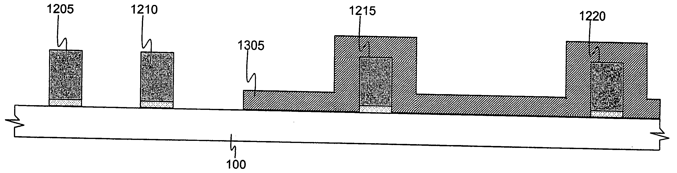
[0029] The invention employs selectively applied thin stressed films, such as tensile films, thin compressive films, and thick tensile films, to enhance electron and hole mobility in CMOS circuits. An exemplary process in accordance with the invention entails steps of applying each film, and patterning for selectively removing the applied film from areas that would not experience performance benefit from the applied stressed film.

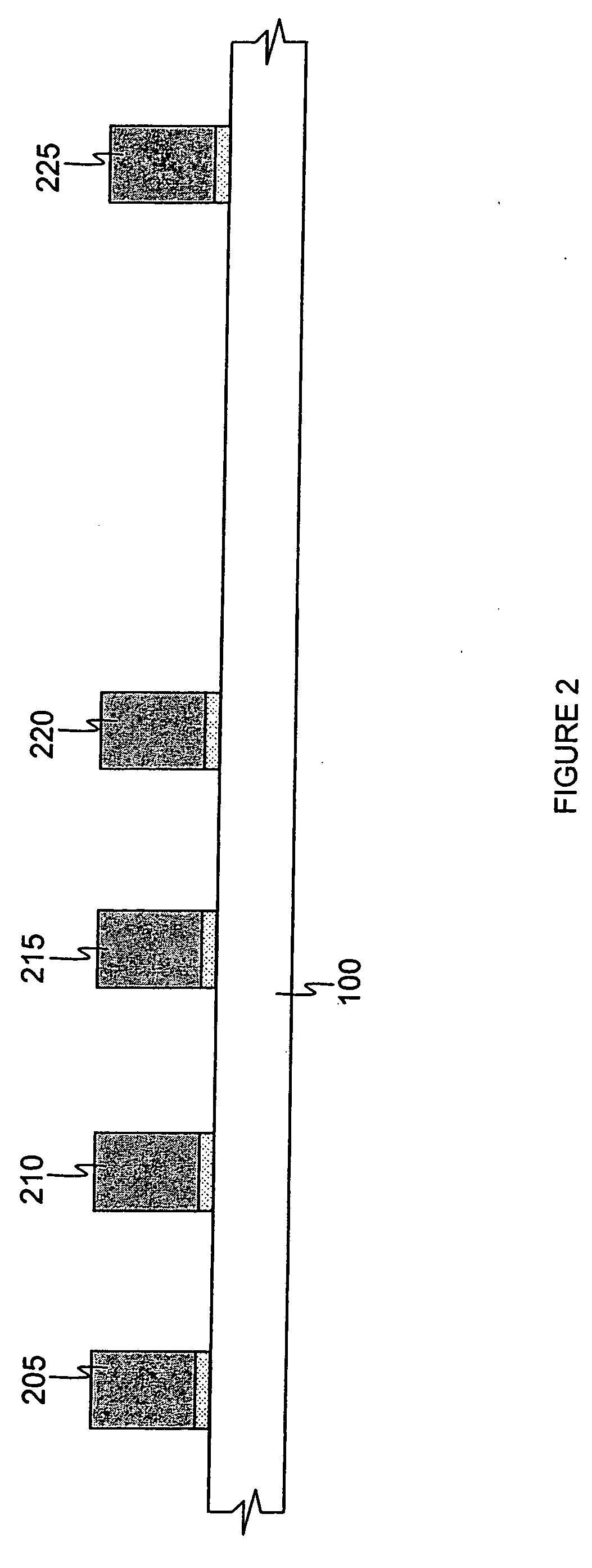
[0030] Referring now to FIG. 1, a substrate 100 having a plurality of FETS (i.e., NFETS and / or PFETS) 105-125 is shown. The substrate 100 includes areas of different densities of nFETS and pFETs, including areas of high concentration or density 130 and areas of low concentration or density 140. Typically, similar devices are clustered; though the invention is applicable to devices having nFETs interspersed with pFETs, and vice versa.

[0031] The high density area 130 exhibits closely spaced FETs. In such an area, the distance from gate to gate may, for exam...


PUM


Abstract

A semiconductor device has selectively applied thin tensile films and thin compressive films, as well as thick tensile films and thick compressive films, to enhance electron and hole mobility in CMOS circuits. Fabrication entails steps of applying each film, and selectively removing each applied film from areas that would not experience performance benefit from the applied stressed film.

Description

BACKGROUND OF THE INVENTION [0001] 1. Field of the Invention [0002] The invention generally relates to a semiconductor device and method of manufacture and, more particularly, to a complementary metal-oxide-semiconductor (CMOS) device that includes an etch stop layer with a selectively varying thickness. [0003] 2. Background Description [0004] As semiconductor devices continue to evolve towards higher densities of circuit elements, the performance of materials used for the devices becomes more critical to overall performance, such as charge carrier mobility. CMOS devices fabricated on substrates having a thin strained silicon (Si) layer on a relaxed SiGe buffer layer exhibit substantially higher electron and hole mobility in strained Si layers than in bulk silicon layers. Furthermore, metal oxide semiconductor field effect transistors (MOSFETs) with strained Si channels exhibit enhanced device performance compared to devices fabricated in conventional (unstrained) silicon substrates...

Claims


Application Information

Patent Timeline
Patent Type & Authority Applications(United States)
IPC IPC(8): H01L21/8238H01L27/01
CPCH01L21/823807H01L29/7842H01L21/823828
Inventor DORIS, BRUCE B.GLUSCHENKOV, OLEG G.ZHU, HUILONG
Owner GLOBALFOUNDRIES INC
Why Eureka
Try Eureka