
Pixel clock creation method, pixel clock creation device, optical scanning device, and image forming apparatus

Inactive Publication Date: 2005-05-12
RICOH KK
View PDF19 Cites 11 Cited by
  • Summary
  • Abstract
  • Description
  • Claims
  • Application Information

AI Technical Summary

Benefits of technology

[0019] An object of the present invention is to provide an improved pixel clock creation method and device in which the above-described problems are eliminated.
[0020] Another object of the present invention is to provide a pixel clock creation method which allows phase control of the pixel clock to be carried out with high precision and simple composition, so that fluctuation of the scanning width can be corrected with high precision.
[0021] Another object of the present invention is to provide a pixel clock creation device which allows phase control of the pixel clock to be carried out with high precision and simple composition, so that fluctuation of the scanning width can be corrected with high precision.
[0025] According to the present invention, the phase control of the pixel clock can be made possible with high precision with simple composition, and it is possible to provide the pixel clock creation device which can correct the fluctuation of the scanning width with high precision.
[0026] Moreover, it is possible to provide the highly precise optical scanning device by incorporating the pixel clock creation device of the invention therein, and it is possible to provide the highly precise image forming apparatus in which the optical scanning device is provided.

Problems solved by technology

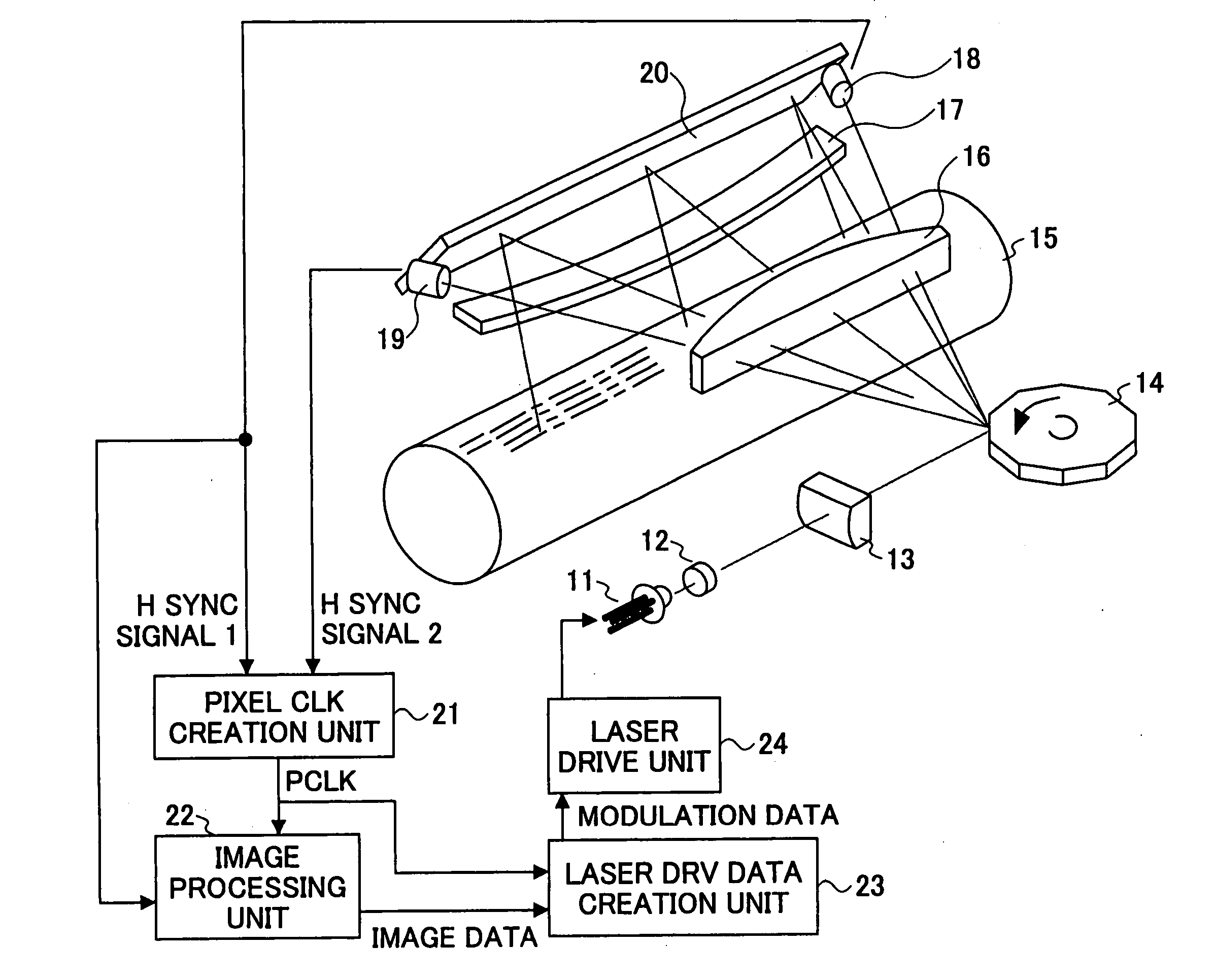
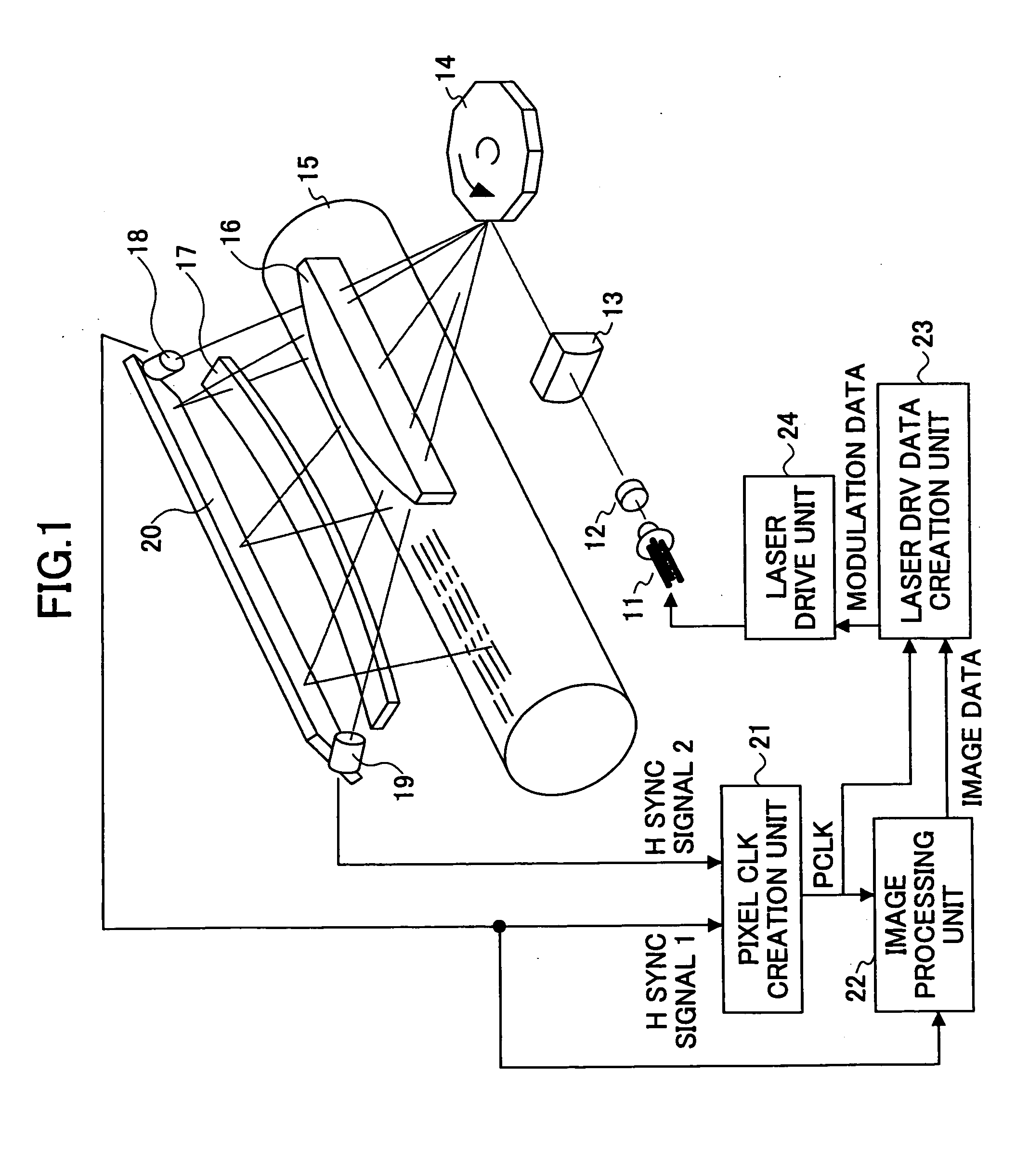
In the above-mentioned scanning optical system, the variations of the distance from the rotation axis of the deflection reflection surface of the deflector, such as the polygon scanner may occur, and the variations may cause the irregularities of the scanning speed of the optical spot (the scanning beam) which optically scans the surface of the photoconductor.
The scanning-speed irregularities may cause fluctuations of the reproduced image, and the image quality will be degraded.
Furthermore, in the case of the multi-beam optical system, when there is a difference in the oscillation wavelength of each of the light sources and the chromatic aberration of the scanning lens is not corrected in the optical system, the deviation of the exposure position occurs.
The difference of the scanning width arises for each of the light sources when the spot corresponding to each source of luminescence scans the surface of the scanned medium, and such difference may cause the degradation of image quality.
It becomes complicated constituting of the image clock control unit the conventional technology (this being called frequency modulation method) of changing the frequency of the image clock.
Moreover, this complexity increases as frequency modulation width becomes minute.
For this reason, there is the problem that fine control cannot be performed, by the conventional frequency modulation method.
Moreover, by the method of controlling the rotary motor of the deflector like the polygon mirror, the limit is in the control accuracy.
Therefore, even if it is the optical beam deflected by the same deviation reflection surface, it is difficult to cancel scanning irregularities, and by the method of controlling the rotary motor of the deflector, the limit is in the control accuracy.

Method used


Image

  • Pixel clock creation method, pixel clock creation device, optical scanning device, and image forming apparatus
  • Pixel clock creation method, pixel clock creation device, optical scanning device, and image forming apparatus
  • Pixel clock creation method, pixel clock creation device, optical scanning device, and image forming apparatus

Examples


first embodiment

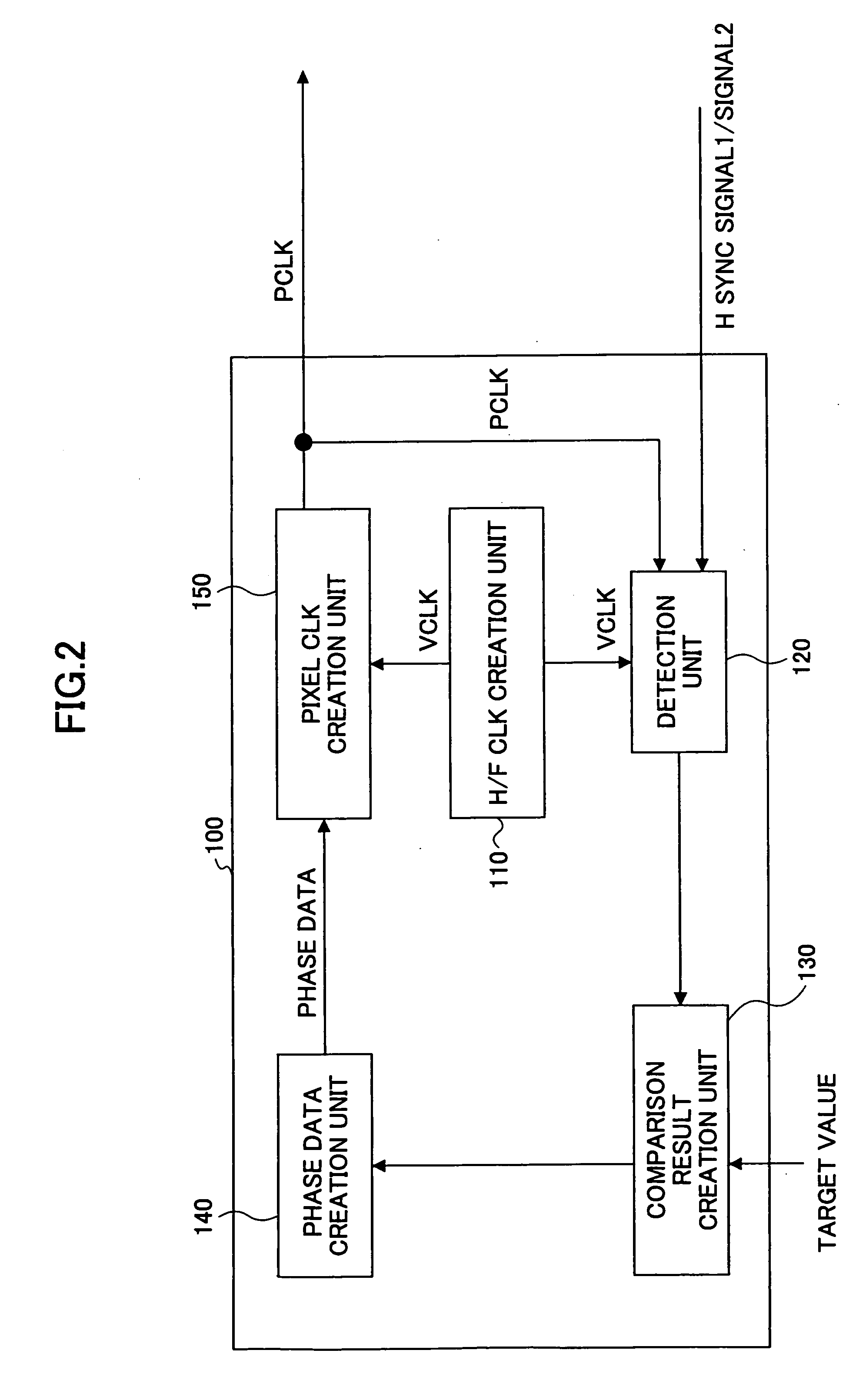
[0164]FIG. 14 is a block diagram of the detection unit 120 in FIG. 2.

[0165] The detection unit 120 comprises the detection data creation circuit 1213 which creates detection data from the output value and horizontal sync signal2 of counter (2) 1212 counted in falling of counter (1) 1211 and the high frequency clock VCLK counted in rising of the high frequency clock VCLK on the basis of the horizontal sync signal1, counter (1) 1211, and counter (2) 1212 in FIG. 14.

[0166]FIG. 15 and FIG. 16 show the case where it falls when the horizontal sync signal1 is in the state of “H” of VCLK.

[0167] Counter (2) 1212 are previously reset by 0 (b of FIG. 15, b of FIG. 16), next counter (1) 1211 are reset by 0 (c of FIG. 15, c of FIG. 16), and the count is carried out by what (a of FIG. 15, a of FIG. 16) the horizontal sync signal1 fell.

[0168] And when the horizontal sync signal2 is in the state of “H” of VCLK and it falls (d of FIG. 15), the count value of counter (1) 1211 and counter (2) 1212 ...

second embodiment

[0176]FIG. 19 is a block diagram of the detection unit 120 in FIG. 2.

[0177] The counter 1221 which counts the detection unit 120 in rising of the high frequency clock VCLK in FIG. 19. State creation circuit (1) 1222 which create the state signal 1 which shows the state of VCLK when the horizontal sync signal1 falls.

[0178] It comprises in the detection data creation circuit 1224 which creates detection data from state creation circuit (2) 1223 which create the state signal 2 of VCLK when the horizontal sync signal2 falls, the count value of the counter 1221, the state signal 1, and the state signal 2.

[0179] The example of composition of state signal creation circuit (1) 1222 is shown in FIG. 20.

[0180] State signal creation circuit (2) The composition of 1223 also becomes the same. The timing view of state signal creation circuit (1) 1222 of operation of FIG. 20 is shown in FIG. 21 and FIG. 22.

[0181]FIG. 21 shows the case where it falls when the horizontal sync signal1 is in the s...

third embodiment

[0202]FIG. 24 is a block diagram of the detection unit in FIG. 2.

[0203] In FIG. 24, the pixel clock PCLK is given from the pixel clock creation circuit 150 synchronizing with falling of the horizontal sync signal1.

[0204] Counter (1) 1231 is a counter which it is reset based on falling of the horizontal sync signal1, and is counted by PCLK. Counter (2) 1232 is a counter which it is reset based on rising of PCLK and counted in rising of the high frequency clock VCLK. Counter (3) 1233 is a counter which it is reset based on rising of PCLK and counted in falling of VCLK.

[0205] The detection data creation circuits 1234 are counter (1) 1231 when the horizontal sync signal2 falls, counter (2) 1232, and the circuit that creates detection data from the value of counter (3) 1233.

[0206] Counter (1) 1231 of FIG. 24, counter (2) 1232, and the timing of counter (3) 1233 of operation are shown in FIG. 25, FIG. 26, and FIG. 27. PCLK uses FIG. 25, FIG. 26, and FIG. 27 as 8 dividing clock of VCLK....


PUM


Abstract

In a pixel clock creation method and device, a high frequency clock is created. A scanning time needed to scan a predetermined scanning length is detected in accuracy of half a period of the high frequency clock to output a detection value indicating the detected scanning time. The detection value and a predetermined target value are compared to output a comparison result. A phase data is created based on the comparison result. A pixel clock whose phase is controlled based on both the high frequency clock and the phase data is created.

Description

BACKGROUND OF THE INVENTION [0001] 1. Field of the Invention [0002] The present invention generally relates to pixel clock creation and phase control widely used in image forming apparatuses including laser printers and digital copiers. More particularly, the present invention relates to a pixel clock creation method and device which realize highly precise phase control of the pixel clock, an optical scanning device and an image forming apparatus equipped with the pixel clock creation device. [0003] 2. Description of the Related Art [0004]FIG. 43 shows the composition of the image forming apparatus, such as laser printer, digital copier etc. [0005] As shown in FIG. 43, the scanning of the laser light which is emitted from the semiconductor laser 501 is carried out by the polygon mirror 502 which is rotated. The laser light from the polygon mirror 502 is focused through the scanning lens 503 and forms the optical spot on the photoconductor 504 which is the scanned medium. The photoco...

Claims


Application Information

Patent Timeline
IPC IPC(8): G02B26/10B41J2/44G02B26/12G06K15/12H04N1/036H04N1/113
CPCG06K15/1219G02B26/127
Inventor NIHEI, YASUHIROISHIDA, MASAAKIOMORI, ATSUFUMIOZASA, DAN
Owner RICOH KK
Learn More