Magnetic device and magnetic memory

a magnetic memory and magnetic field technology, applied in the field of magnetic devices and magnetic memory, can solve the problems of difficult localization of magnetic fields, insufficient magnetic field generation, and high reversal current for reversing magnetization

Active Publication Date: 2005-05-12
KATANA SILICON TECH LLC
View PDF19 Cites 53 Cited by
  • Summary
  • Abstract
  • Description
  • Claims
  • Application Information

AI Technical Summary

Benefits of technology

[0015] the ferromagnetic coupling having a strength such that a parallel magnetic alignment of the magnetic layers is maintained when the write current is passed.

Problems solved by technology

However, magnetic field is difficult to localize because it basically has the nature of spreading out into space.
An attempt to select a bit or cell of a microscopic size for controlling its magnetization direction encounters a “crosstalk” problem of erroneously selecting a nearby bit or cell, or otherwise a great problem that a smaller source for generating magnetic field cannot generate sufficient magnetic field.
However, the “current-driven magnetization reversal” has a problem at present that reversal current for reversing magnetization is extremely high, as much as 10 mA to several mA.

Method used


Image

  • Magnetic device and magnetic memory
  • Magnetic device and magnetic memory
  • Magnetic device and magnetic memory

Examples


first embodiment

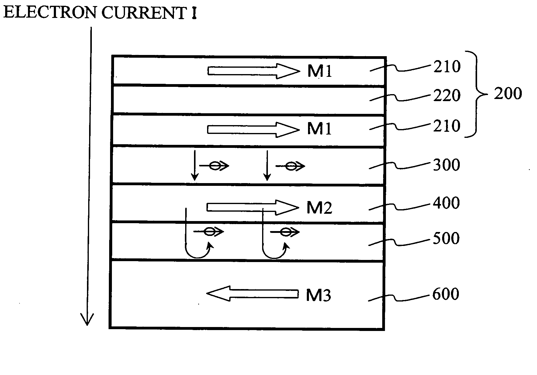
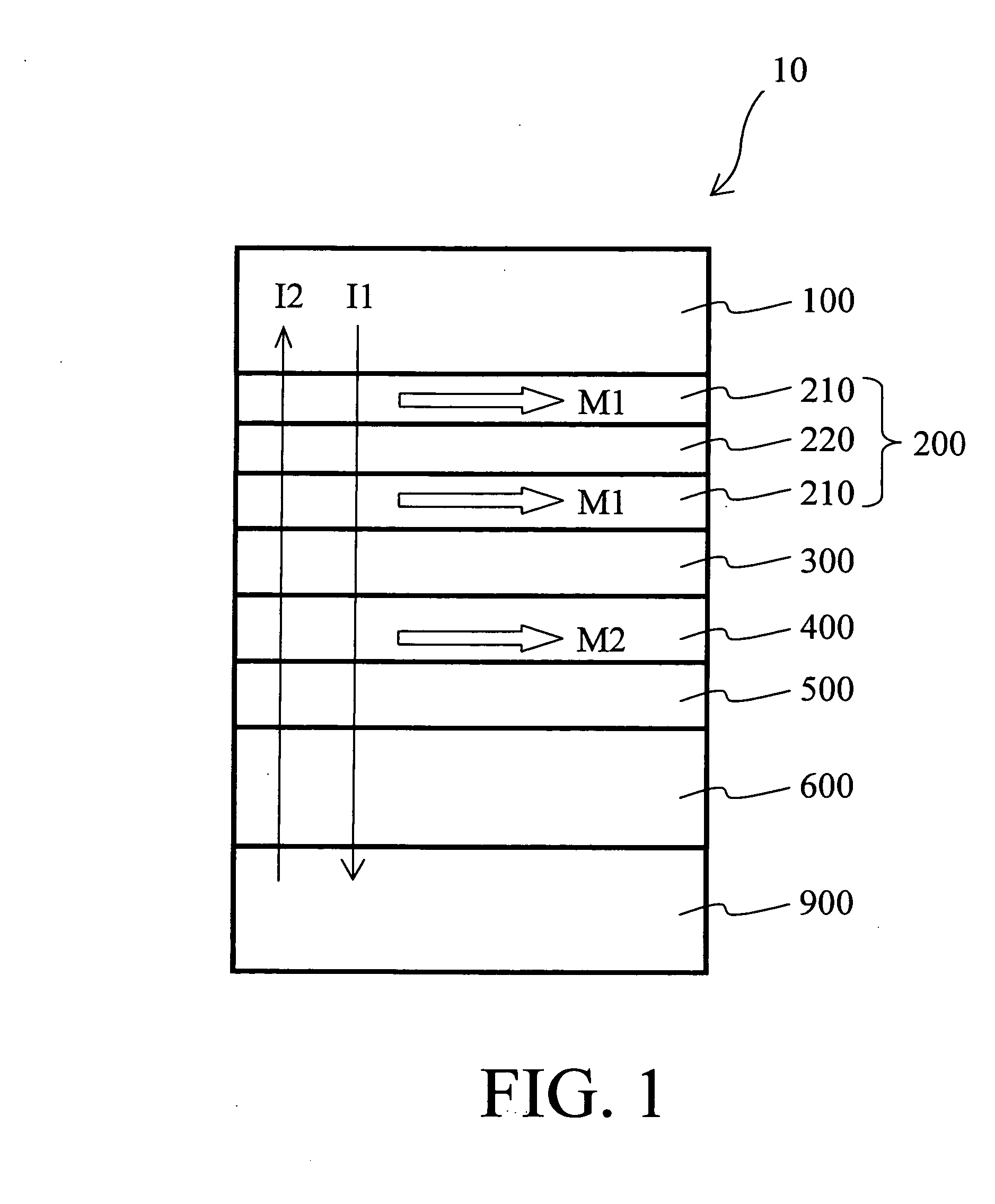
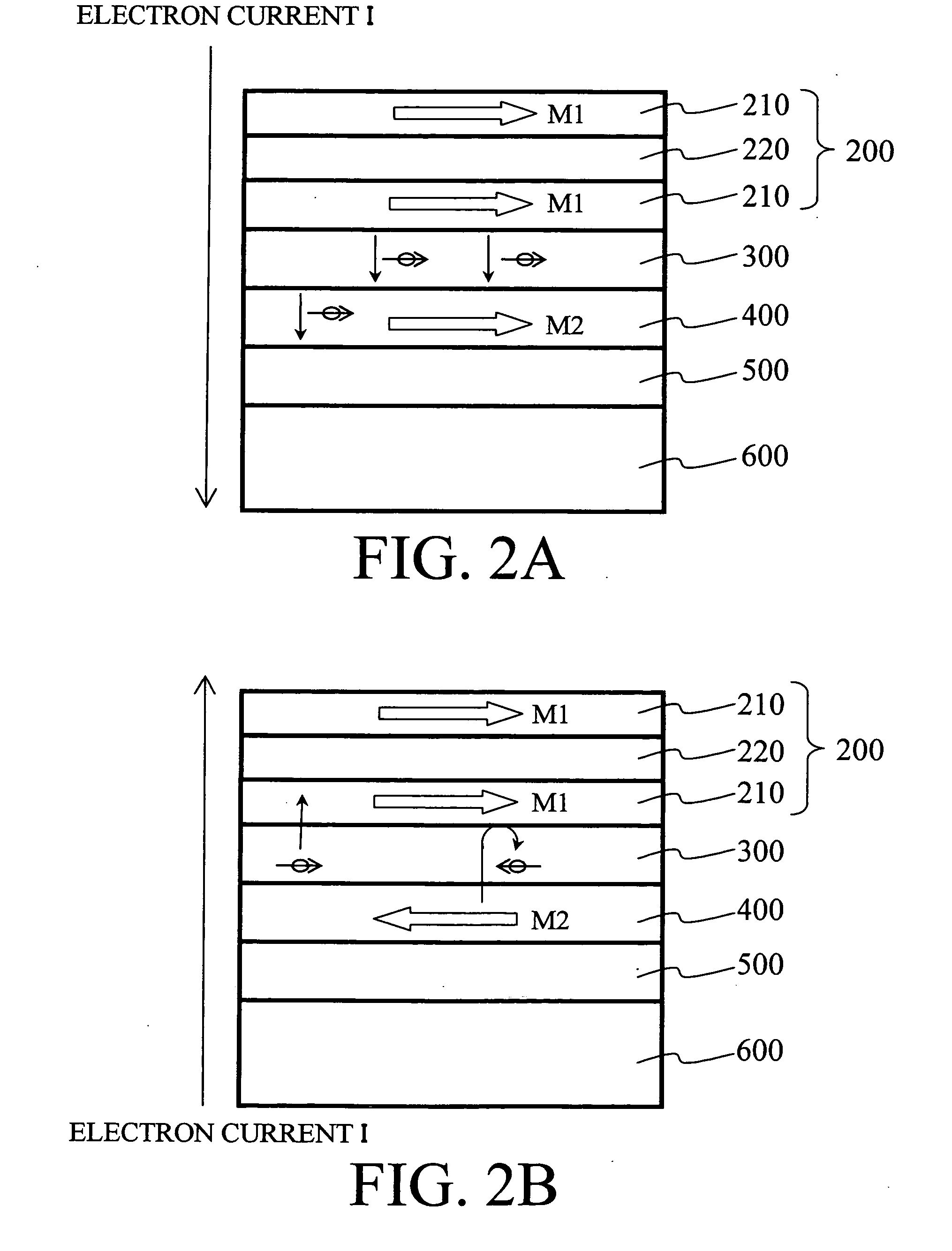
[0083]FIG. 1 is a schematic view illustrating a basic cross-sectional structure of a magnetic device according to a first embodiment of the invention. The magnetic device 10 is configured such that a first pinned layer 200, first intermediate layer 300, free layer 400, second intermediate layer 500 and second pinned layer 600 are stacked between a couple of electrodes 100 and 900 configured to provide write current between the first and second ferromagnetic layers to cause spin-polarized electrons to act on the third ferromagnetic layer so that the direction of magnetization of the third ferromagnetic layer is determined depending on a direction of the current.

[0084] The first pinned layer 200 comprises a multilayer film in which at least two magnetic layers are ferromagnetically coupled with each other. Each of these magnetic layers has an easy axis of magnetization substantially parallel to the film plane. The multilayer film is composed of (magnetic layer 210 / nonmagnetic layer 2...

second embodiment

[0138] Next, as a second embodiment of the invention, a magnetic device will be described in which the free layer 400 is multilayered.

[0139]FIG. 15 is a schematic view illustrating a basic cross-sectional structure of a magnetic device according to a second embodiment of the invention. In this figure, the same elements as those previously described with reference to FIGS. 1 to 14 are given the same reference numerals and not described in detail.

[0140] In this embodiment, the free layer 400 is configured as a multilayer film composed of (magnetic layer 410 / nonmagnetic layer 420)×N / magnetic layer 410 (N=1 or greater) that are ferromagnetically coupled. That is, the free layer 400 is configured such that magnetic layers 410 and nonmagnetic layers 420 are stacked alternately with each other, and that magnetic layers 410 are ferromagnetically coupled with each other via a nonmagnetic layer 420 having a enough coupling strength such that the magnetization of the free layer 400 rotates m...

third embodiment

[0154] Next, as a third embodiment of the invention, a magnetic device will be described in which the first pinned layer 200 and the free layer 400 are each multilayered.

[0155]FIG. 17 is a schematic view illustrating a basic cross-sectional structure of a magnetic device according to a third embodiment of the invention. In this figure again, the same elements as those previously described with reference to FIGS. 1 to 16 are given the same reference numerals and not described in detail.

[0156] In this embodiment, the first pinned layer 200 and the free layer 400 are each configured as a multilayer film composed of (magnetic layer / nonmagnetic layer)×N / magnetic layer (N=1 or greater) that are ferromagnetically coupled. That is, the first pinned layer 200 is configured such that magnetic layers 210 and nonmagnetic layers 220 are stacked alternately with each other, and that at least two of the magnetic layers 210 are ferromagnetically coupled via a nonmagnetic layer 220. Likewise, the ...


PUM

PropertyMeasurementUnit
thicknessaaaaaaaaaa
reversal currentaaaaaaaaaa
thicknessaaaaaaaaaa

Abstract

A magnetic device comprises first through third ferromagnetic layers, first and second intermediate layers and a couple of electrodes. The first ferromagnetic layer includes magnetic layers and one or more nonmagnetic layers which are alternately stacked, at least one layer of the magnetic layers has magnetization substantially fixed to a first direction, and two or more layers of the magnetic layers are ferromagnetically coupled via the nonmagnetic layers while having easy axes of magnetization parallel to a film plane. The second ferromagnetic layer has magnetization substantially fixed to a second direction. The third ferromagnetic layer is provided between the first ferromagnetic layer and the second ferromagnetic layer. The third ferromagnetic layer has a variable direction of magnetization. The first and second intermediate layers are provided between the ferromagnetic layers. The electrodes are configured to provide write current between the first and second ferromagnetic layers to cause spin-polarized electrons to act on the third ferromagnetic layer so that the direction of magnetization of the third ferromagnetic layer is determined depending on a direction of the current. The ferromagnetic coupling has a strength such that a parallel magnetic alignment of the magnetic layers is maintained when the write current.

Description

CROSS-REFERENCE TO RELATED APPLICATIONS [0001] This application is based upon and claims the benefit of priority from the prior Japanese Patent Application No. 2003-342576, filed on Sep. 30, 2003; the entire contents of which are incorporated herein by reference. BACKGROUND OF THE INVENTION [0002] The invention relates to a magnetic device and a magnetic memory, and in particular, to a magnetic device having recording and reproducing capability and to a magnetic memory using the same. [0003] A conventional method of controlling the magnetization direction of magnetic material is to apply an external magnetic field. For example, in a hard disk drive, a magnetic field generated from a recording head reverses the magnetization direction of the magnetic recording medium to perform write operation. In a solid magnetic memory, electric current generated in a wire placed in the vicinity of a magnetoresistance effect device produces a current-induced magnetic field, which is applied to a ce...

Claims


Application Information

Patent Timeline
Patent Type & Authority Applications(United States)
IPC IPC(8): G11B5/127G11B5/39G11C11/15H01L21/8246H01L27/105H01L43/00H01L43/08
CPCG11C11/15G11B5/1276
Inventor NAKAMURA, SHIHOHANEDA, SHIGERU
Owner KATANA SILICON TECH LLC
Why Eureka
Try Eureka