Chip-on-film package for image sensor and method for manufacturing the same

a technology of image sensor and chip, which is applied in the direction of semiconductor devices, electrical equipment, semiconductor/solid-state device details, etc., can solve the problems of difficult sealing, high cost, and difficulty in making electrically double-sided conductive traces on transparent glass, and achieve the effect of simplifying the filling material

Inactive Publication Date: 2005-05-19
ADVANCED SEMICON TECH
View PDF3 Cites 59 Cited by
  • Summary
  • Abstract
  • Description
  • Claims
  • Application Information

AI Technical Summary

Benefits of technology

[0016] In the third embodiment of the present invention, as showed in FIG. 4, components disclosed in another COF package for image sensor which are same or similar to those used in the first embodiment are presented by the same elements number, such as transparent glass 20, image sensing chip 30. The COF package for image sensor includes a COF film 50, an image sensing chip 30 and a transparent glass 20. The COF film 50 comprises an electrically insulating layer 51 and a plurality of metal traces 55. The metal traces 55 are formed on the lower surface 53 of the electrically insulating layer 51 and each metal trace 55 connects a flip-chip connect pad 56 on the upper surface 52 of the electrically insulating layer 51 by passing through via. The flip-chip connect pads 56 are disposed around the opening 54 and substantially attached to the electrically insulating layer 51. The image sensing chip 30 is flip-chip mounted on the upper surface 52 of the C

Problems solved by technology

The transparent glass has to be pervious to light and has double-sided electrical conduction, but it is difficult and costs high to make electrically double-sided conductive traces on the transparent glass.
However, the size of the image-sensing chip is almost same as that of the transparent layer, so that the sealer is difficult to form by dispensing after electrically connecting the image sensing chip with the transp

Method used


Image

  • Chip-on-film package for image sensor and method for manufacturing the same
  • Chip-on-film package for image sensor and method for manufacturing the same
  • Chip-on-film package for image sensor and method for manufacturing the same

Examples


Embodiment Construction

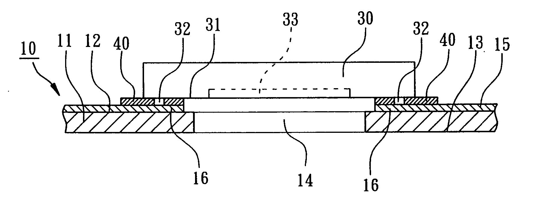
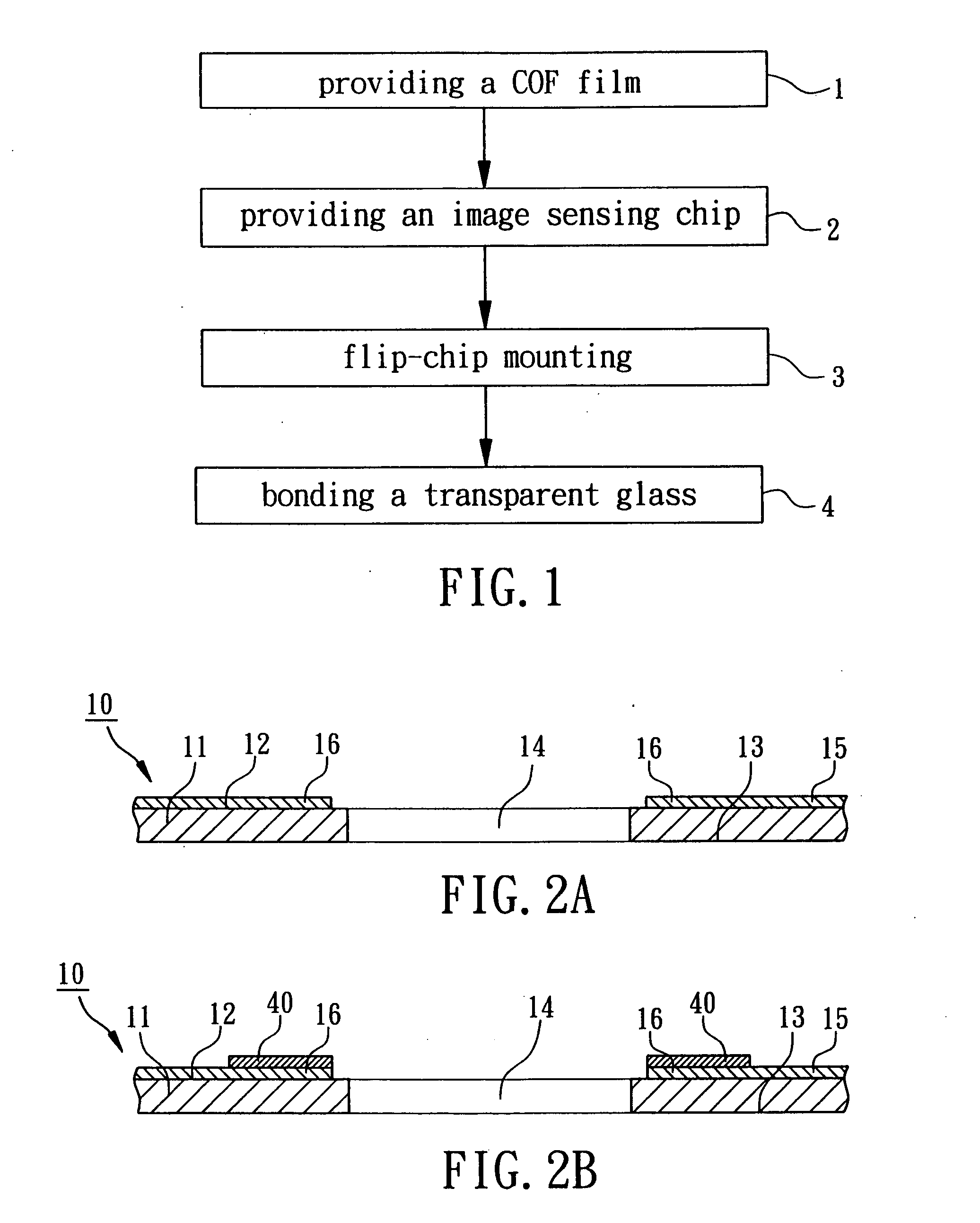
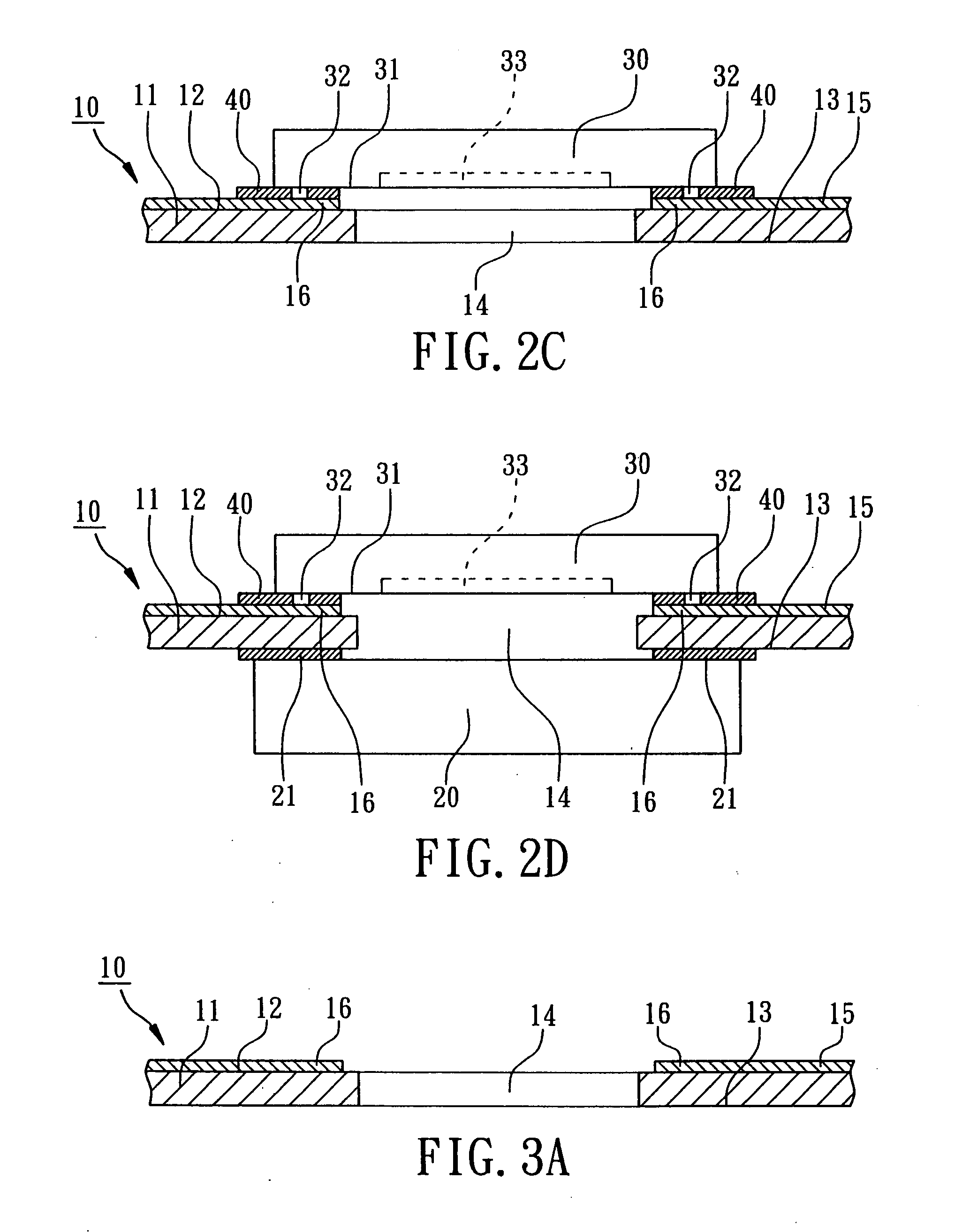
[0013] Referring to the drawings attached, the present invention will be described by means of the embodiments below. According to the first embodiment of the present invention, as showed in FIG. 1, a method for manufacturing a chip-on-film package for image sensor includes a step 1 of “providing a COF film”, a step 2 of “providing an image sensing chip”, a step 3 of “flip-chip mounting” and a step 4 of “bonding a transparent glass”. The chip-on-film package for image sensor as showed in FIG. 2D is manufactured by COF tape package manufacturing process. The chip-on-film package for image sensor includes a COF film 10 with wiring pattern. The COF film 10 is obtained from a COF tape that can be rolled up and conveyed by reel to reel. The COF film 10 includes an insulating layer 11 and a plurality of metal traces 15. The insulating layer 11 is flexible and electrically insulating and has a thickness approximately several ten micrometers. The insulating layer 11, is made of polyimide, p...


PUM


Abstract

A chip-on-film (COF) package and method for image sensor has been disclosed. According to the method a COF film with opening is provided. The COF film has an upper surface, a lower surface and at least an opening. An image sensing chip is flip-chip mounted on the upper surface of the COF film. A transparent glass is bonded to the lower surface of the COF film. The opening is clipped by the transparent glass and the image sensing chip to form a hermetic space. The active surface of the image sensing chip includes an image sensing region toward the transparent glass through the opening and is sealed in the hermetic space by a limited filling material in order to prevent the image sensing region of the image sensing chip from contamination by means of COF tape packaging method.

Description

FIELD OF THE INVENTION [0001] The present invention is relating to a package for image sensor, particularly to a chip-on-film package for image sensor and method for manufacturing the same. BACKGROUND OF THE INVENTION [0002] Conventional image sensor includes a semiconductor chip with image sensing function (it will be abbreviated as image sensing chip below) for sensor of charge coupled device (CCD) or complementary metal oxide semiconductor (CMOS). The active surface of the image sensing chip is relatively sensitive to dust, so that it needs to be protected with a suitable package from invasion by dust and moisture. Conventional method for packaging image sensing chip is firstly to carry an image sensing chip on a hard medium such as leadframe or printed circuit board, then to be sealed by a glass cover and a dam. Practically, the leadframe or printed circuit board in plate-shape or strip-shape for image sensing chip shall be hard enough to form the dam during packaging process. [...

Claims


Application Information

Patent Timeline
IPC IPC(8): H01L21/56H01L31/0203
CPCH01L21/563H01L27/14618H01L31/0203H01L2224/16225H01L2224/32225H01L2224/73204H01L2924/00
Inventor YANG, CHARLESKUO, ALLEN
Owner ADVANCED SEMICON TECH
Why Eureka
Try Eureka