
Manufacturing method of semiconductor device

a manufacturing method and semiconductor technology, applied in the direction of semiconductor devices, electrical devices, transistors, etc., can solve the problems of poor contact, unstable substrate potential, lowered surface concentration of p-type impurity diffusion region, etc., to achieve easy control of implantation energy, suppress diffusion progress, and suppress variation of element concentration profile

Active Publication Date: 2005-05-19
SEMICON COMPONENTS IND LLC
View PDF6 Cites 0 Cited by
  • Summary
  • Abstract
  • Description
  • Claims
  • Application Information

AI Technical Summary

Benefits of technology

The present invention provides a manufacturing method for a semiconductor device that includes a high melting point metal layer. The method includes steps of forming an element region with a p-type impurity diffusion region and an n-type channel layer on a semiconductor substrate, and then sequentially forming an interlayer insulating film with a contact hole, a metal wiring layer, and a source region and body region on the element region. The method also includes steps of ion-implanting a p-type impurity into the contact hole and diffusing the impurity through the contact hole to form a high melting point metal layer in contact with the source region and body region through the contact hole. The method helps to maintain the impurity concentration in the vicinity of the surface of the substrate and suppress the variation of the concentration profile in the element region, which can lead to improved performance and reliability of the semiconductor device.

Problems solved by technology

Thus, there have been problems that grains (silicon nodules) of silicon mixed in aluminum to suppress spike (mutual diffusion of aluminum and silicon) block up the source region or the body region exposed in the contact hole CH, and poor contact occurs or the substrate potential becomes unstable.
However, there has been a problem that at the time of this reaction, boron atoms in the element region formed in the silicon substrate are absorbed by the titanium silicide layer and the surface concentration of the p-type impurity diffusion region is lowered.
As stated above, when the surface concentration of the body region is lowered, the substrate potential can easily become unstable, and there is a problem that deterioration of avalanche resistance is caused.
As stated above, when the source region 35 is extended, the channel region formed along the trench 27 becomes short, and there has been a problem that the increase of IDSS leak and the deterioration of VDSS are caused by the short channel effect.

Method used


Image

  • Manufacturing method of semiconductor device
  • Manufacturing method of semiconductor device
  • Manufacturing method of semiconductor device

Examples


Embodiment Construction

[0066] Embodiments of the present invention will be described in detail with reference to FIGS. 1 to 14.

[0067] First, a first embodiment of the invention will be described with reference to FIGS. 1 to 8 while a MOSFET of a p-channel trench structure is used as an example.

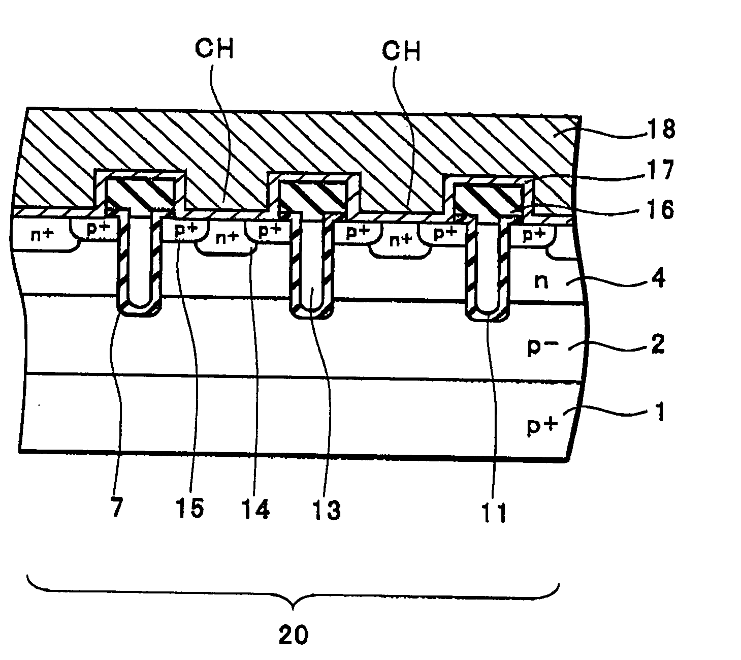
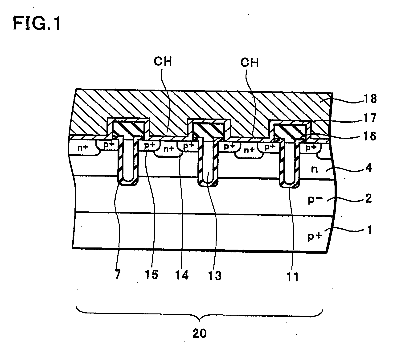
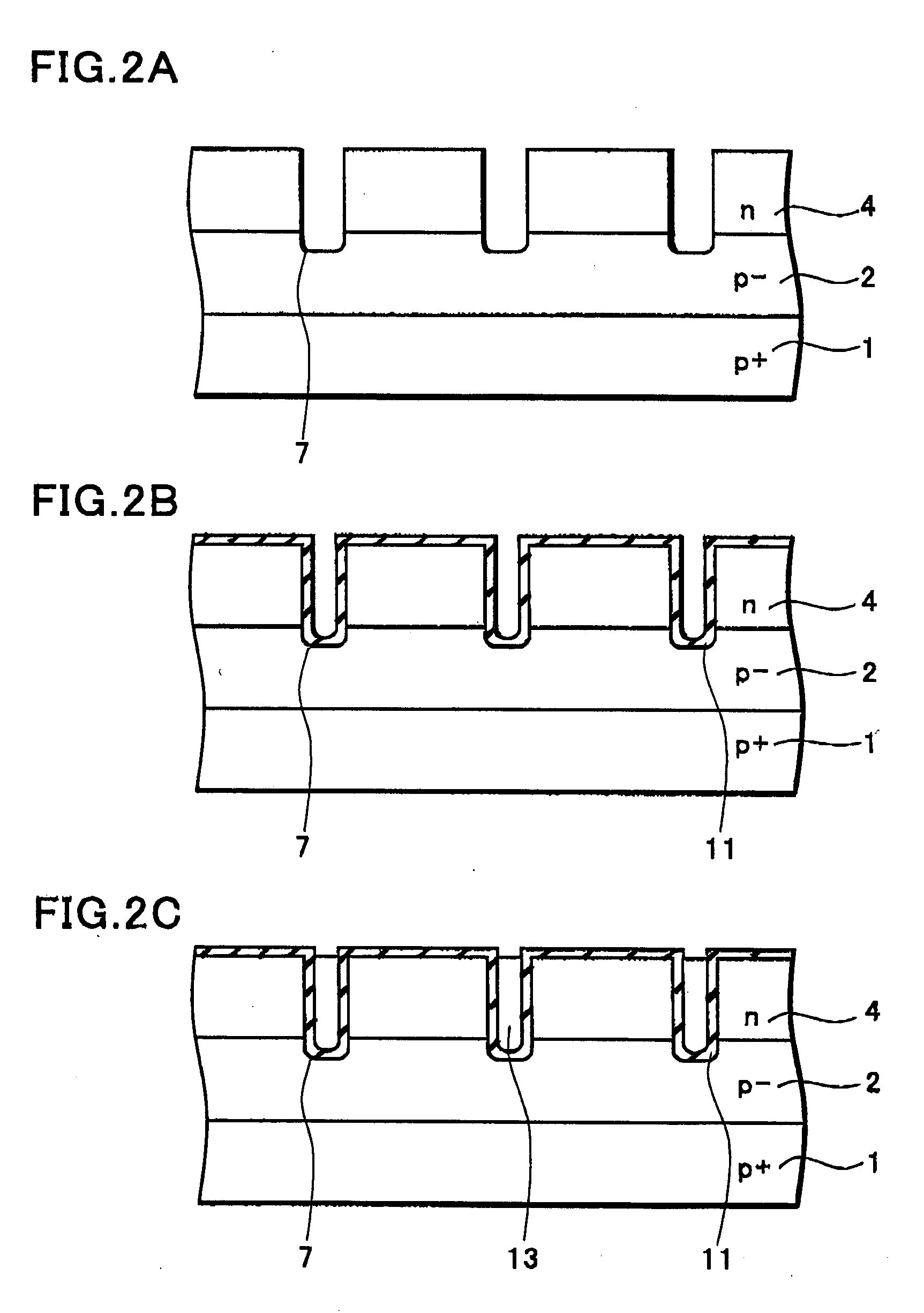
[0068]FIG. 1 shows a structure of the trench type MOSFET of the invention. A drain region 2 made of a p−-type epitaxial layer is provided on a p+-type silicon semiconductor substrate 1, and an n-type channel layer 4 is provided on its surface.

[0069] Trenches 7 are provided to pass through the channel layer 4 and to reach the drain region 2, an inner wall of each of the trenches 7 is coated with a gate oxide film 11, and a gate electrode 13 made of polysilicon filled in the trench 7 is provided.

[0070] P+-type source regions 15 are provided on the surface of the channel layer 4 adjacent to the trench 7, and an n+-type body region 14 is disposed on the surface of the channel layer 4 between the source regions 15 of...


PUM

PropertyMeasurementUnit
melting pointaaaaaaaaaa
temperatureaaaaaaaaaa
melting pointaaaaaaaaaa

Abstract

When Ti as a barrier metal layer is brought into contact with a diffusion region of boron provided on a surface of a silicon substrate, there is a problem that boron is absorbed by titanium silicide, and contact resistance is increased. Although there is a method of additionally implanting boron whose amount is equal to the amount of boron absorbed by titanium silicide, there has been a problem that when boron is additionally implanted into, for example, a source region in a p-channel type, the additionally added boron is diffused deeply at the diffusion step, and characteristics are deteriorated. According to the invention, after formation of an element region, boron is additionally implanted into the whole surface at a dosage of about 10% of an element region, and is activated in the vicinity of a surface of a silicon substrate by an alloying process of a barrier metal layer. By this, a specified concentration profile of the element region is kept, and the impurity concentration only in the vicinity of the surface can be raised. Accordingly, even if boron is absorbed by titanium silicide, a specified boron concentration can be kept in the element region, and the increase of contact resistance can be suppressed.

Description

BACKGROUND OF THE INVENTION [0001] 1. Field of the Invention [0002] The present invention relates to a manufacturing method of a semiconductor device, and particularly to a manufacturing method of a semiconductor device in which the increase of contact resistance due to the absorption of boron by titanium is suppressed and the characteristics are improved. [0003] 2. Description of the Related Art [0004] As the miniaturization of a semiconductor device advances, in the semiconductor device with a silicon substrate, a barrier metal layer made of titanium-based metal (for example, Ti, TiN, TiON, TiW, etc.) is formed before the formation of a wiring layer. [0005] With reference to FIGS. 15 to 17, a conventional manufacturing method of a semiconductor device will be described while a power MOSFET with a trench structure is used as an example. [0006] In FIG. 15, a p−-type epitaxial layer is laminated on a p+-type silicon semiconductor substrate 21 to form a drain region 22. After an oxide...

Claims


Application Information

Patent Timeline
Patent Type & Authority Applications(United States)
IPC IPC(8): H01L21/28H01L21/00H01L21/04H01L21/335H01L21/336H01L21/82H01L27/02H01L29/417H01L29/423H01L29/45H01L29/49H01L29/72H01L29/772H01L29/78
CPCH01L29/7813H01L29/456H01L21/02244H01L21/02579H01L21/22H01L29/0843H01L29/0856H01L29/49H01L2924/01005H01L2924/01022H01L2924/13091
Inventor KUBO, HIROTOSHIIGARASHI, YASUHIROSHIBUYA, MASAHIRO
Owner SEMICON COMPONENTS IND LLC
Learn More