Diffusion barriers formed by low temperature deposition

a technology of diffusion barriers and low temperature, applied in the direction of semiconductor devices, semiconductor/solid-state device details, electrical equipment, etc., can solve the problems of increasing the resistivity of films, process may not be compatible with a variety of otherwise useful dielectric materials, and the potential of damaging the dielectric wiring structur

Inactive Publication Date: 2005-05-26
IBM CORP
View PDF25 Cites 65 Cited by
  • Summary
  • Abstract
  • Description
  • Claims
  • Application Information

AI Technical Summary

Benefits of technology

[0008] A solid state device includes a first material and a second material. A barrier layer is formed between the first material and the second material to prevent diffusion between the first material and the second material. The barrier laye

Problems solved by technology

If the temperature required to deposit a film with useful barrier properties is greater than about 400 degrees C., the process may not be compatible with a variety of otherwise useful dielectric materials, as these materials may not be chemically stable at these elevated temperatures.
Even if the dielectric is chemically stable, the high temperature excursion has the potential of damaging the dielectric wiring structure at least through thermal expansion coefficient mismatches between the metal wiring struc

Method used


Image

  • Diffusion barriers formed by low temperature deposition
  • Diffusion barriers formed by low temperature deposition
  • Diffusion barriers formed by low temperature deposition

Examples


Embodiment Construction

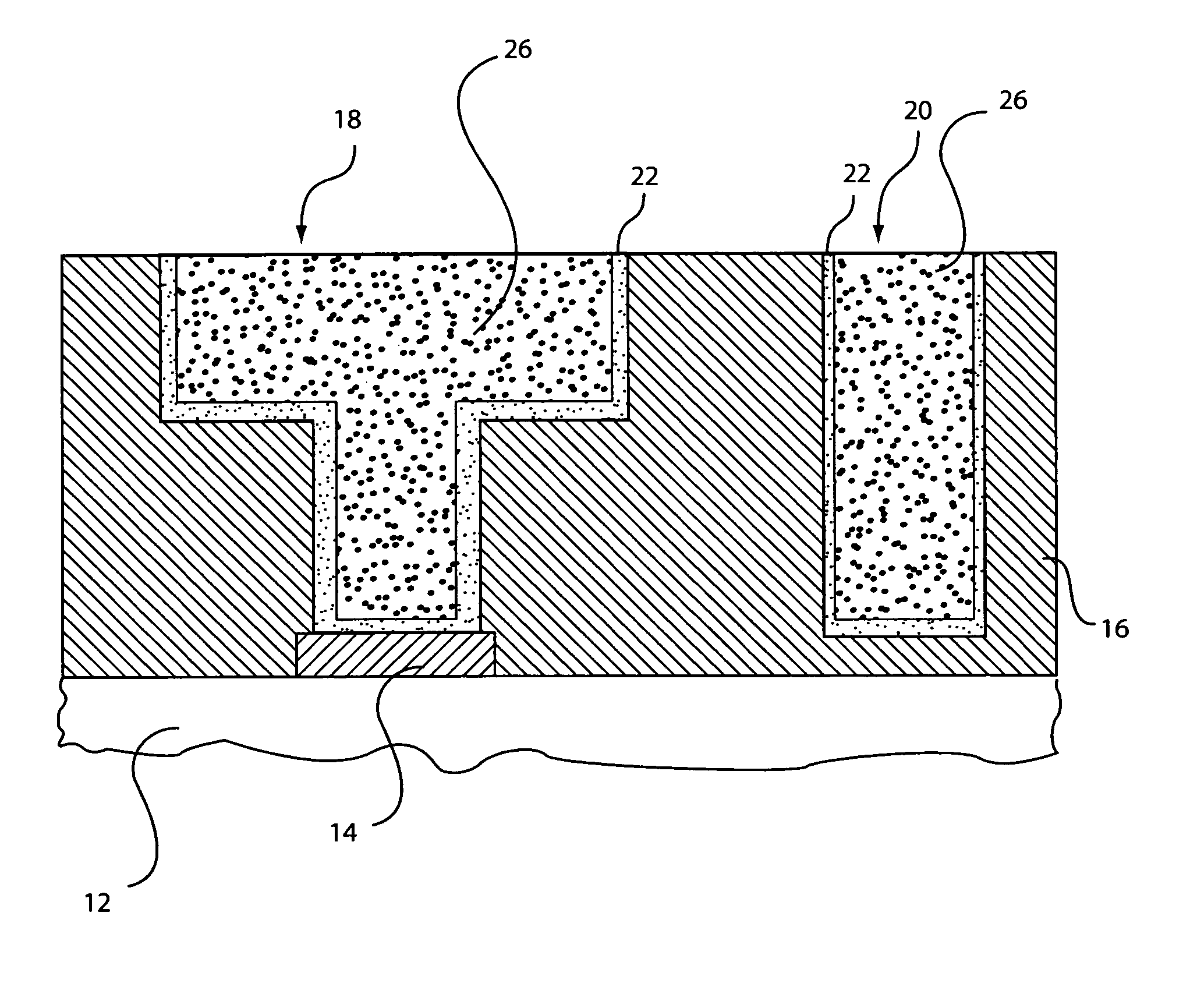
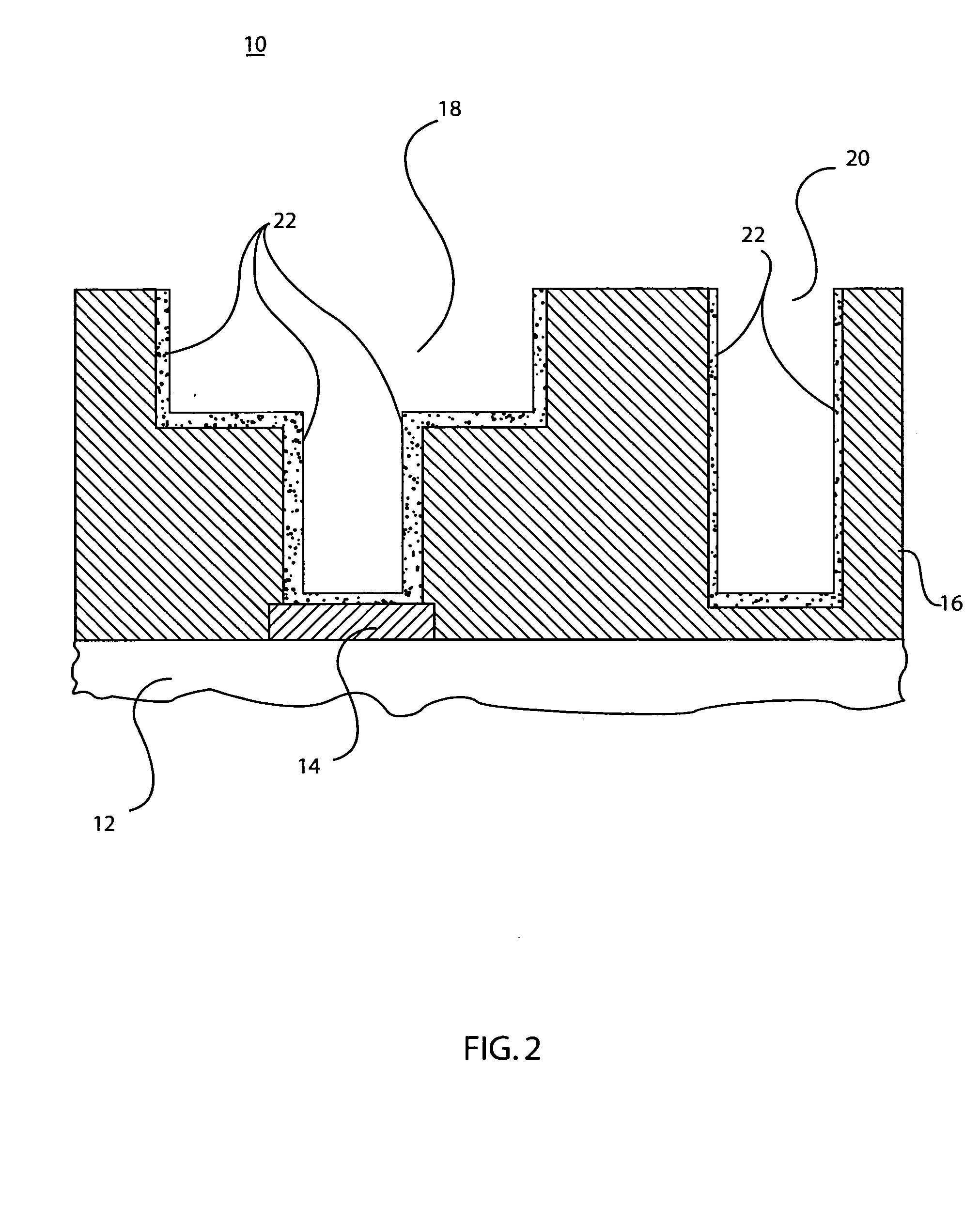
[0016] The present invention provides a diffusion barrier, which is formable at low temperatures, e.g., below 400 degrees C., and preferably below 350 degrees C. For feature sizes below about 0.1 microns, chemical vapor deposition (CVD) may be employed for the fabrication barrier layers since CVD provides high inherent conformality. In one embodiment, a copper conductor may be employed with a barrier film interface. The barrier is formed from Ru or Re compounds and can be at least at least as low in resistance than barrier films made from Tungsten (W) while being deposited at a substantially lower temperature. In addition, barrier layers made from Ru or Re have a much higher tolerance to processing effects for example, adhesion to the dielectric is maintained after additional process steps are performed than W films deposited at the corresponding low temperature.

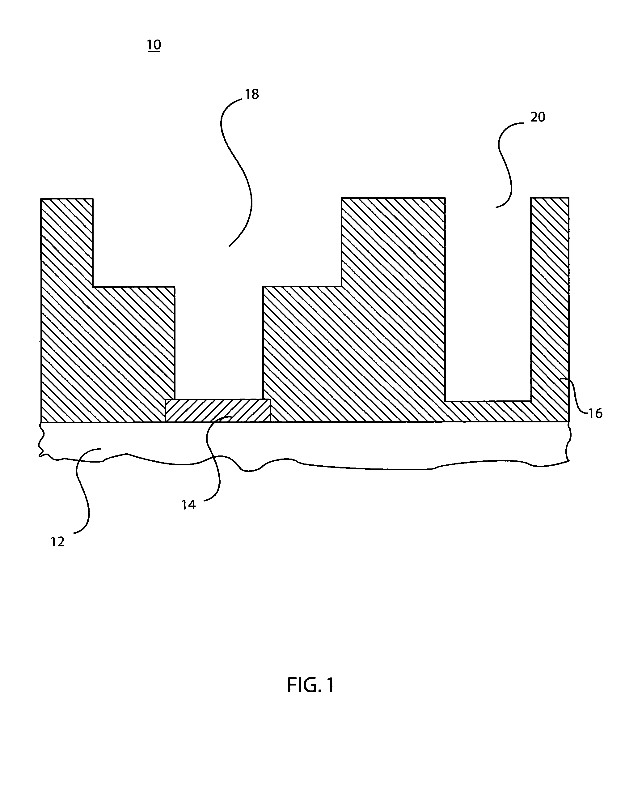
[0017] It should be understood that FIGS. 1-3 show an illustrative semiconductor or solid state device structure to demon...


PUM


Abstract

A solid state device includes a first material and a second material. A barrier layer is formed between the first material and the second material to prevent diffusion between the first material and the second material. The barrier layer includes a metal form of at least one of Ru and Re. The barrier layer is preferably formed using a low temperature deposition process, where the substrate is less than 400 degrees C.

Description

BACKGROUND OF THE INVENTION [0001] 1. Field of the Invention [0002] This invention relates to forming diffusion barriers, and more particular to devices and methods for forming diffusion barriers for wiring structures in semiconductor devices by depositing thin metallic films using chemical vapor deposition (CVD). [0003] 2. Description of the Related Art [0004] Diffusion barriers are employed in semiconductor fabrication processes to reduce diffusion or the exchange of atoms between two regions. For example, copper wiring for integrated microelectronic circuit technology may use a diffusion barrier material to prevent the diffusion of the copper, which forms wires, into a matrix of dielectric where the wires are embedded. [0005] To produce metal films of usable quality for diffusion barriers, a substrate must be subjected to elevated temperatures during deposition. If the temperature required to deposit a film with useful barrier properties is greater than about 400 degrees C., the ...

Claims


Application Information

Patent Timeline
IPC IPC(8): H01L21/285H01L21/4763H01L21/768H01L23/48H01L23/532H01L29/40
CPCH01L21/28556H01L21/76843H01L23/53223H01L23/53238H01L2924/0002H01L23/53252H01L2924/00
Inventor LANE, MICHAEL WAYNELAVOIE, CHRISTIAN C.MALHOTRA, SANDRA G.MCFEELY, FENTON R.YURKAS, JOHN JACOB
Owner IBM CORP
Why Eureka
Try Eureka