Semiconductor device

a technology of semiconductors and semiconductors, applied in the direction of semiconductor devices, electrical equipment, transistors, etc., can solve the problems of difficult mounting of mixed-mount transistors, easy formation of parametric transistors, and easy operation, and achieve the effect of simplifying manufacturing processes

Active Publication Date: 2005-06-02
SILTERRA MALAYSIA SDH BHD +1
View PDF6 Cites 19 Cited by
  • Summary
  • Abstract
  • Description
  • Claims
  • Application Information

AI Technical Summary

Benefits of technology

[0012] Impurity formation is not only performed for channel stopper in the present invention (at the same time as source and drain formation), and therefore manufacturing processes can be simplified. Further, one STI element isolator can be used as an element isolator for microscopic transistors of an LVMOS transistor region, and therefore it is possible to compactly mount them mixedly with the LVMOS transistors having a gate length in the sub-micron order.

Problems solved by technology

In particular, parasitic transistors are easily formed, and easily operated, in wirings used for HVMOS transistor regions because a high voltage is normally applied.
In addition, a large area is necessary for the element isolators used with the Locos because of the Locos bird's beak region, and it is difficult to mount them mixedly with the LVMOS transistors having gate lengths in a sub-micron order compactly.

Method used


Image

  • Semiconductor device
  • Semiconductor device
  • Semiconductor device

Examples


Embodiment Construction

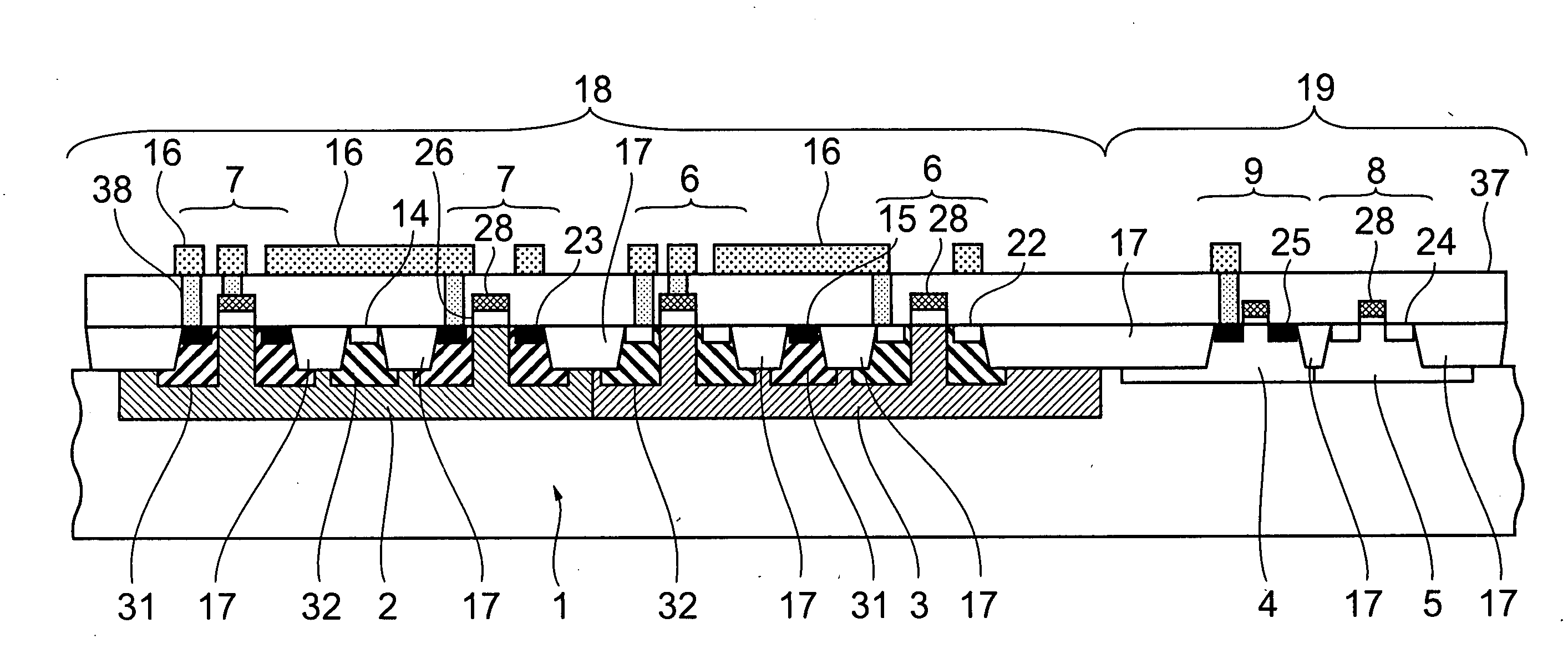
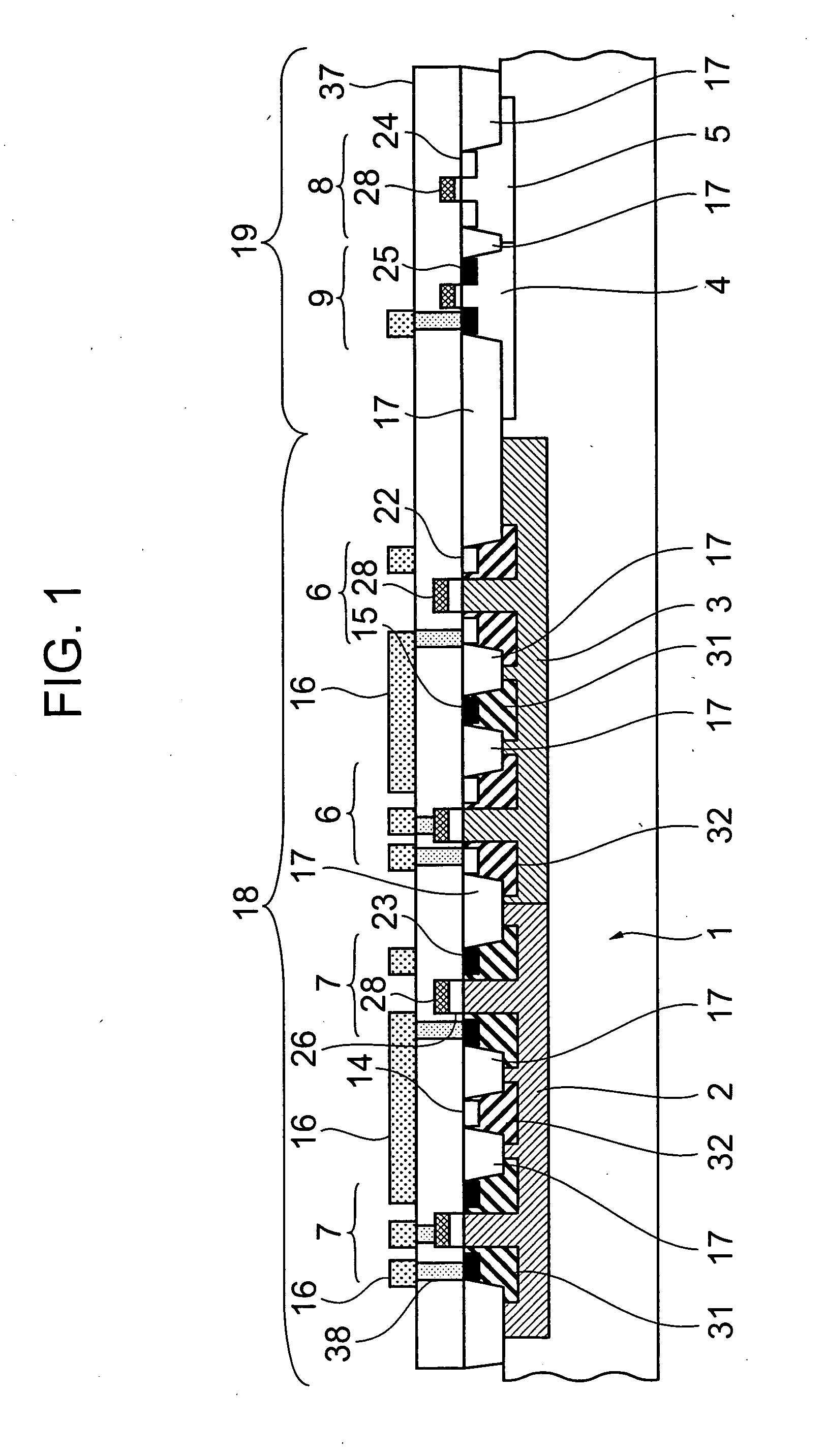
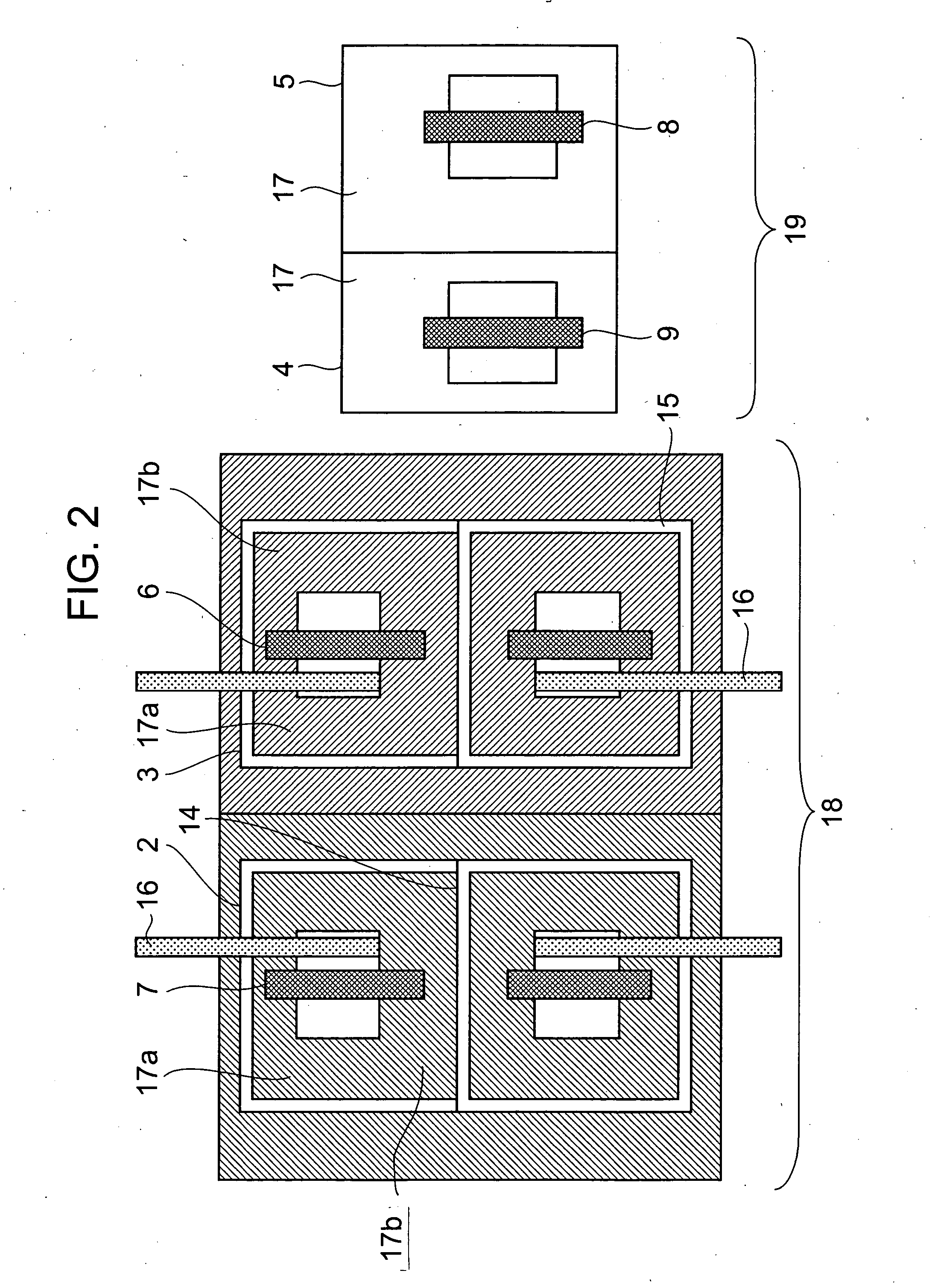
[0024]FIG. 1 is a cross sectional diagram of a structure of an embodiment of the present invention and the embodiment will be explained below. An HVNwell 2 and an HVPwell 3 formed within an HV region 18 for forming a high voltage (HV) MOS transistor, and an LVNwell 4 and an LVPwell 5 formed within an LV region 19 for forming an LVMOS transistor, are disposed on an Si substrate 1. Elements are isolated within each of the HVPMOS and HVNMOS transistor element formation regions 18 by two STIs 17. Elements are isolated with each of the LVPMOS and LVNMOS transistor element formation regions 19 by the one STI 17.

[0025] The HVNwell 2 is an HVMOS formation region, and an n-type conductivity impurity region. The HVPwell 3 is an HVMOS formation region, and a p-type conductivity impurity region. The LVNwell 4 is an LVMOS formation region, and an n-type conductivity impurity region. The LVPwell 5 is an LVMOS formation region, and a p-type conductivity impurity region.

[0026] A plurality of p-ch...


PUM


Abstract

In a semiconductor device in which high voltage MOS transistors and low voltage MOS transistors are mixedly mounted, a process is simplified and miniaturization thereof is achieved, without causing a parasitic transistor operation. An active region doped with a low impurity concentration of an impurity is formed in a channel region of a parasitic MOS transistor between two STI (shallow trench isolation) regions, and current flow between a source and a drain of the parasitic MOS transistor is cut off in a semiconductor device in which a high voltage MOS transistor and a microscopic low voltage MOS transistor are mixedly mounted on the same semiconductor substrate.

Description

BACKGROUND OF THE INVENTION [0001] 1. Field of the Invention [0002] The present invention relates to a semiconductor device in which high voltage MOS (hereinafter referred to as HVMOS) transistors and low voltage MOS (hereinafter referred to as LVMOS) transistors are mixedly mounted and formed on the same semiconductor substrate. HVMOS transistors are transistors normally used for driving liquid crystal display devices or thermal heads, and their operation voltage and output voltage are from 8 V to 50 V. Further, LVMOS transistors normally refer to transistors having a gate length in a sub-micron order, which are manufactured with a process rule of 0.25 μm or less, their operation voltage is on the order of 0.9 to 3.3 V, and they are applied in memory and logic circuits. [0003] 2. Description of the Related Art [0004] In conventional techniques, element isolators are formed in order to isolate mutually adjacent transistors when a plurality of high voltage (HV) MOS transistors are fo...

Claims


Application Information

Patent Timeline
Patent Type & Authority Applications(United States)
IPC IPC(8): H01L21/76H01L21/762H01L21/8234H01L21/8238H01L27/08H01L27/088H01L27/092H01L29/76
CPCH01L21/76237H01L27/0921H01L21/823878H01L21/823814
Inventor INOUE, NAOTOSAKURAI, HITOMIPAEK, MINKIM, SANG YEONKIM, IN KI
Owner SILTERRA MALAYSIA SDH BHD
Why Eureka
Try Eureka