Bipolar transistor

a transistor and bipolar technology, applied in the field of bipolar transistors, can solve the problems of low activation rate of mg, low hole mobility, and high base resistance rsub>b /sub>, and achieve the effect of high current gain

Inactive Publication Date: 2005-06-02
SHARP KK
View PDF3 Cites 6 Cited by
  • Summary
  • Abstract
  • Description
  • Claims
  • Application Information

AI Technical Summary

Benefits of technology

[0009] Accordingly, an object of this invention is to provide a bipolar transistor, which has a structure whose performance is not influenced by the sheet resistance of the base layer and is able to exhibit a high current gain even in a high-frequency region.

Problems solved by technology

However, in the III-N compound semiconductor, the activation rate of Mg is low, and the mobility of holes is low.
Therefore, the conventional HBT has a problem that the base resistance rb becomes high, and the power gain is low in the high-frequency region.

Method used


Image

  • Bipolar transistor
  • Bipolar transistor
  • Bipolar transistor

Examples


first embodiment

The First Embodiment

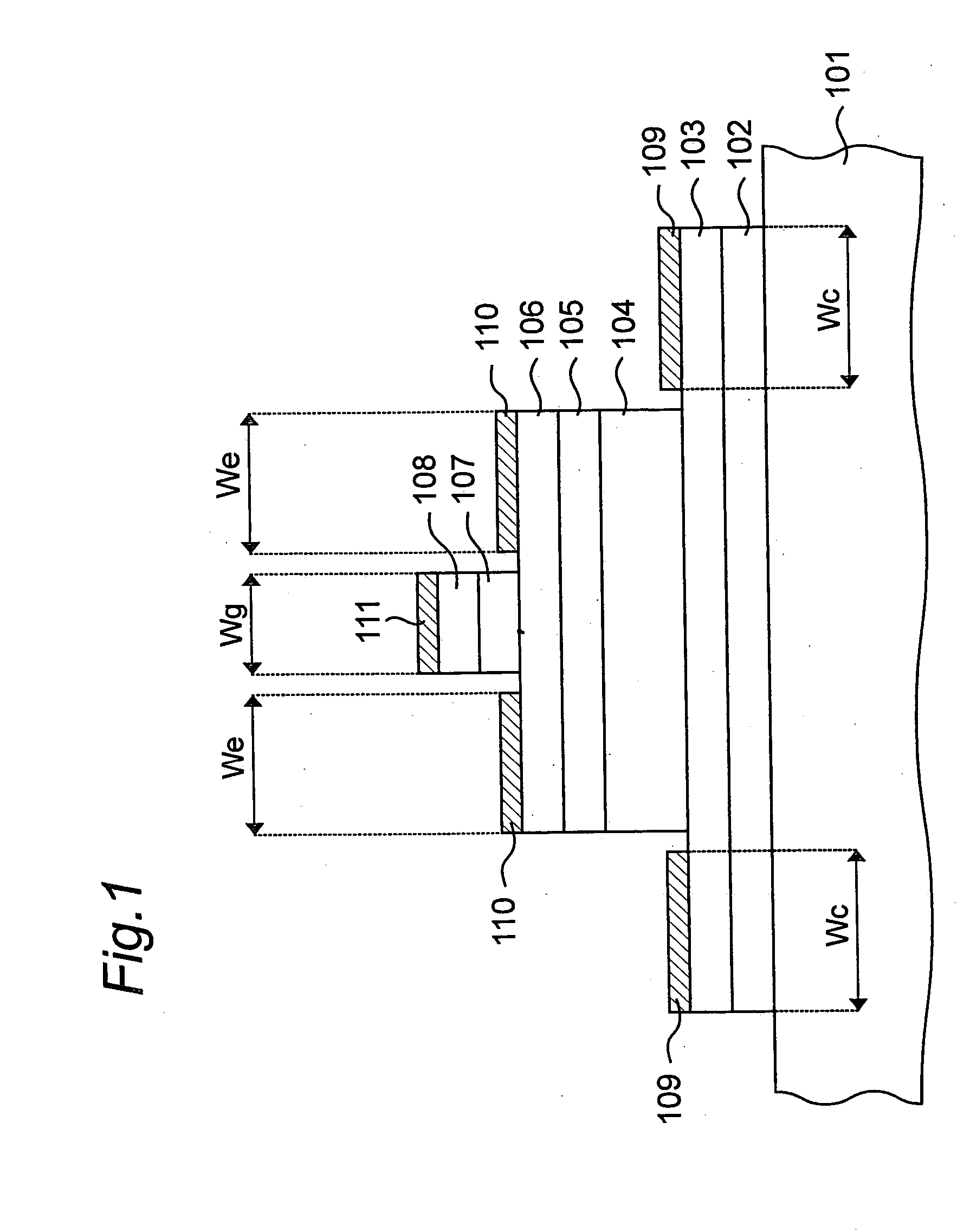
[0085]FIG. 7 shows the cross-sectional structure of the device of the first embodiment to which this invention is applied.

[0086] This device is provided with an n-GaN subcollector layer (layer thickness: 100 nm, Nd=5×1018 cm−3) 703, an n-InxGa1-xN collector layer (layer thickness: 500 nm, In composition ratio x=0→0.2, Nd=1×1016 cm−3) 704 formed in a central region of the upper surface of this subcollector layer 703, a p-In0.2Ga0.8N base layer (layer thickness: 25 nm, Na=5×1019 cm3) 705 that serves as a second conductive type carrier retaining layer, an n-GaN emitter layer (layer thickness: 80 nm, Nd=5×1018 cm−3) 706 and a p-Al0.2Ga0.8N gate layer (layer thickness: 50 nm, Na=5×1018 cm−3) 707 formed in a central region of the upper surface of this emitter layers 706. The In crystal mixture ratio x of the n-InxGa1-xN collector layer 704 is graded so that x=0 on the subcollector layer side and x=0.2 on the base layer side. The collector layer 704 is also called the ...

second embodiment

The Second Embodiment

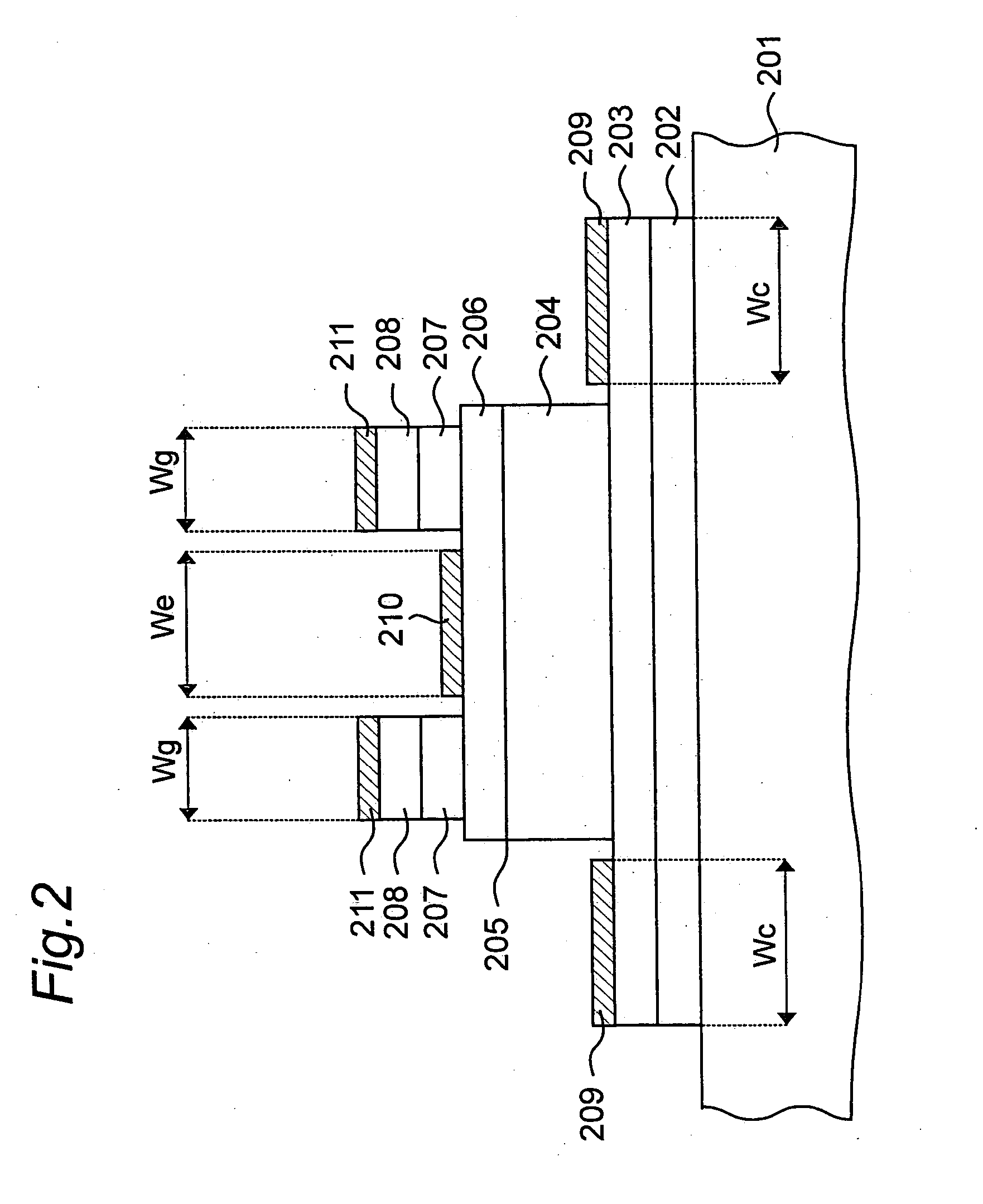
[0097]FIG. 10 shows the cross-sectional structure of the device of the second embodiment to which this invention is applied.

[0098] This device is provided with an n-GaN subcollector layer (layer thickness: 100 nm, Nd=5×1018 cm−3) 1003, an n-InxGa1-xN collector layer (layer thickness: 500 nm, In composition ratio x=0→0.2, Nd=1×1016 cm−3) 1004 formed in a central region of the upper surface of this subcollector layer 1003, an n-GaN emitter layer (layer thickness: 80 nm, Nd=5×1018 cm−3) 1006 and a p-Al0.2Ga0.8N gate layer (layer thickness: 50 nm, Na=5×1011 cm−3) 1007 formed in a central region of the upper surface of this emitter layer 1006. The In crystal mixture ratio x of the n-InxGa1-xN collector layer 1004 is graded so that x=0 on the subcollector layer side and x=0.2 on the emitter layer side.

[0099] A collector electrode 1009, an emitter electrode 1010 and a gate electrode 1011 are formed similarly to those of the first embodiment. The collector electrode 1...

third embodiment

The Third Embodiment

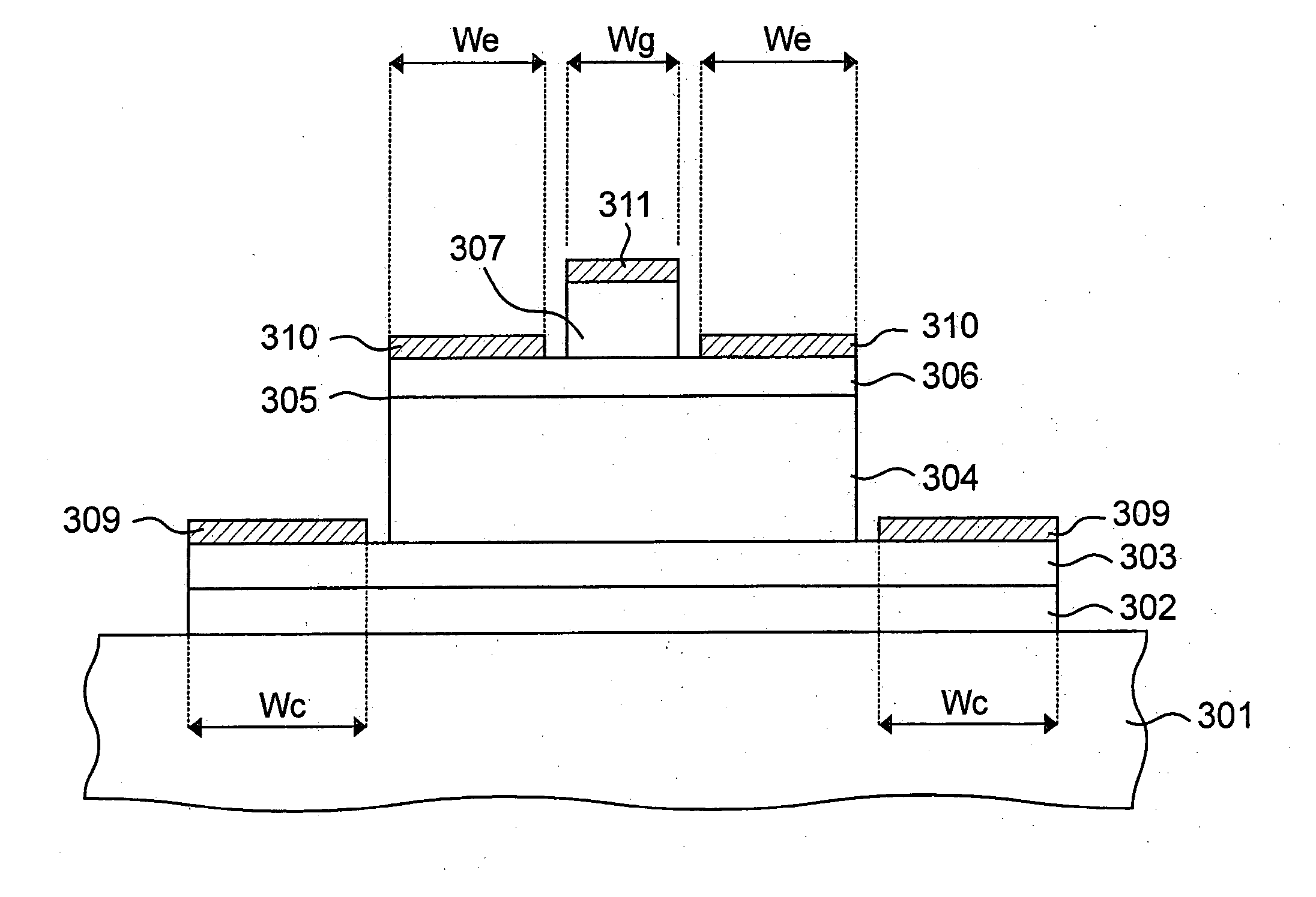
[0108]FIG. 12 shows the cross-sectional structure of the device of the third embodiment to which this invention is applied.

[0109] This device is provided with an n-GaN subcollector layer (layer thickness: 100 nm, Nd=5×1018 cm−3) 1203, an n-InxGa1-xN collector layer (layer thickness: 500 nm, In composition ratio x=0→0.2, Nd=1×1016 cm−3) 1204 formed in a central region of the upper surface of this subcollector layer 1203, an n-GaN emitter layer (layer thickness: 80 nm, Nd=5×1018 cm3) 1206 and an AlxGa1-xN gate layer (layer thickness: 25 nm, Al composition ratio x=0.1→0.3, undoped) 1207 formed in a central region of the upper surface of this emitter layer 1206. The In crystal mixture ratio x of the n-InxGa1-xN collector layer 1204 is graded so that x=0 on the subcollector layer side and x=0.2 on the emitter layer side. Moreover, the Al crystal mixture ratio x of the AlxGa1—N gate layer 1207 is graded so that x=0.1 on the emitter layer side and x=0.3 on the upper su...


PUM


Abstract

A bipolar transistor of the present invention comprises a collector layer made of an n-type semiconductor and an emitter layer made of an n-type semiconductor provided on this collector layer. A gate layer for injecting p-type carriers (holes) into the emitter layer is provided on the emitter layer. A p-type carrier retaining layer is formed between the collector layer and the emitter layer. The p-type carrier retaining layer temporarily retains the p-type carriers that are injected from the gate layer into the emitter layer and diffused in the emitter layer and reach the p-type carrier retaining layer. The bipolar transistor has a structure whose performance is not influenced by sheet resistance of the base layer, and is able to exhibit a high current gain even in a high-frequency region.

Description

[0001] This nonprovisional application claims priority under 35 U.S.C. §119(a) on Patent Application Nos. P2003-399025 and P2004-323844 respectively filed in Japan on Nov. 28, 2003 and Nov. 8, 2004, the entire contents of which are hereby incorporated by reference. BACKGROUND OF THE INVENTION [0002] The present invention relates to bipolar transistors and, in particular, to a bipolar transistor that includes a compound semiconductor of a group III element and nitrogen (N) as a material. [0003] As a type of bipolar transistor that includes a compound semiconductor of a group III element and nitrogen (N) as a material, there is known an HBT (heterojunction bipolar transistor) made of a gallium nitride / aluminum gallium nitride (GaN / AlGaN) material (refer to JP 2002-368005 A). [0004] The HBT is provided with an n+-gallium nitride (GaN) subcollector layer (thickness: ˜1000 nm, silicon (Si) concentration as an n-type dopant: ˜6×1018 cm−3), an n-GaN collector layer formed in a central regi...

Claims


Application Information

Patent Timeline
Patent Type & Authority Applications(United States)
IPC IPC(8): H01L29/08H01L21/331H01L29/20H01L29/737H01L29/76
CPCH01L29/0817H01L29/7606H01L29/7371H01L29/2003
Inventor TWYNAM, JOHN KEVIN
Owner SHARP KK
Why Eureka
Try Eureka