
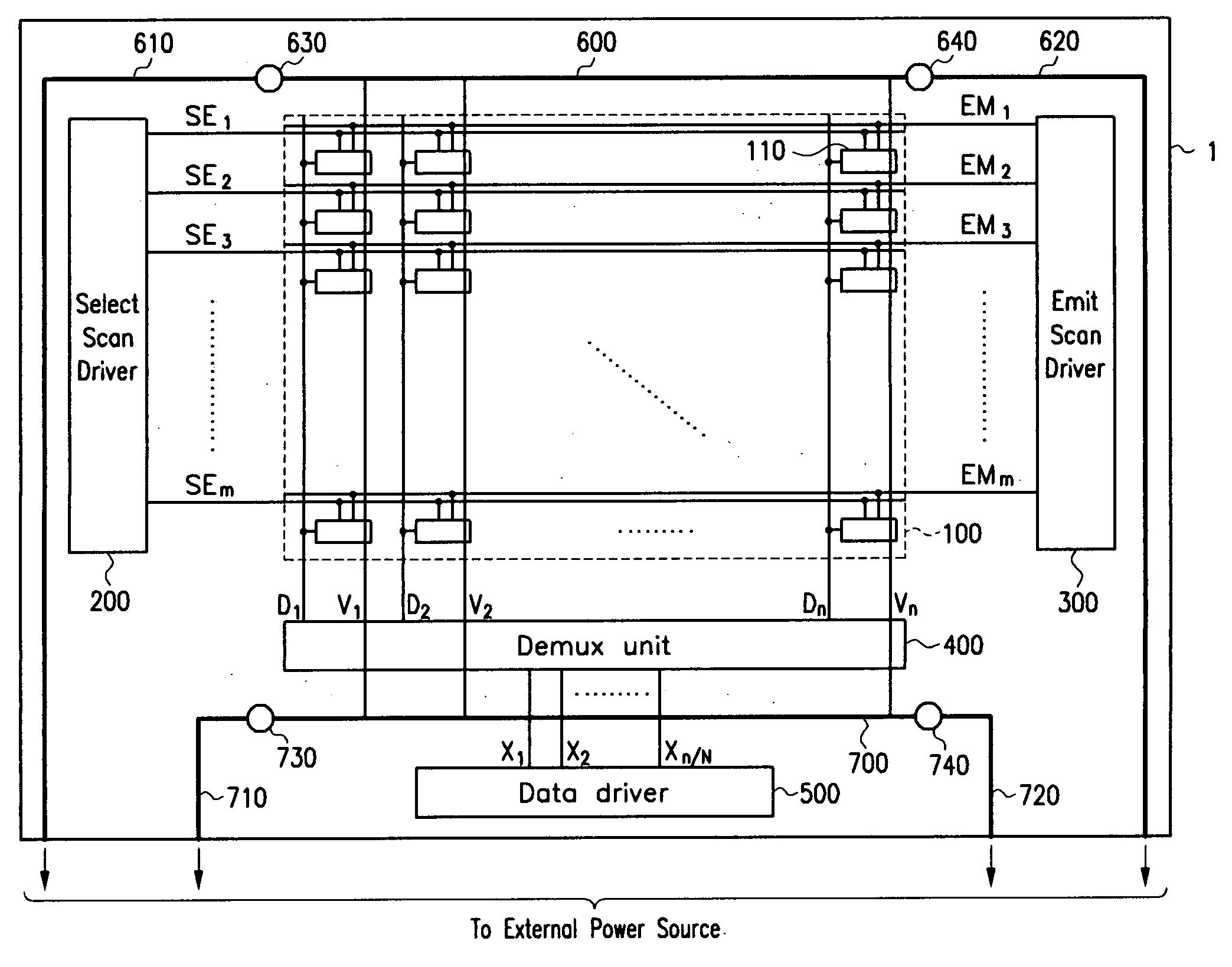
Display device using demultiplexer and driving method thereof

a display device and multi-plexer technology, applied in multiplex communication, static indicating devices, instruments, etc., can solve the problems of shortening the sampling time, hindering the appropriate sampling of data current, increasing power consumption, etc., and achieve the effect of reducing the voltage drop

Inactive Publication Date: 2005-06-02
SAMSUNG DISPLAY CO LTD
View PDF33 Cites 28 Cited by
  • Summary
  • Abstract
  • Description
  • Claims
  • Application Information

AI Technical Summary

Benefits of technology

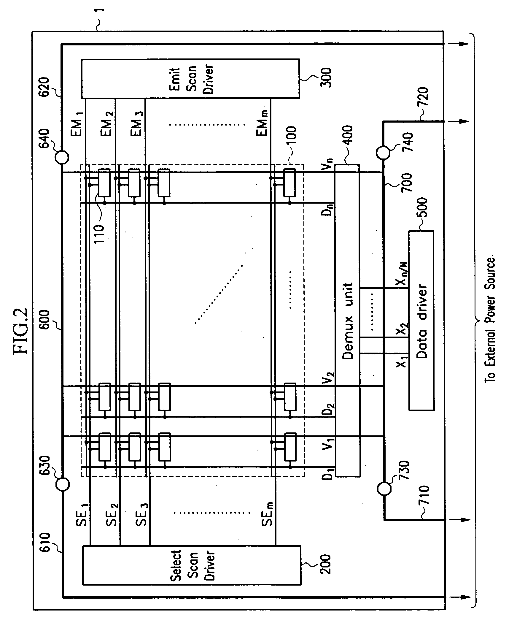
[0011] According to one embodiment, the present invention provides a display device using a demultiplexer for reducing a voltage drop.

Problems solved by technology

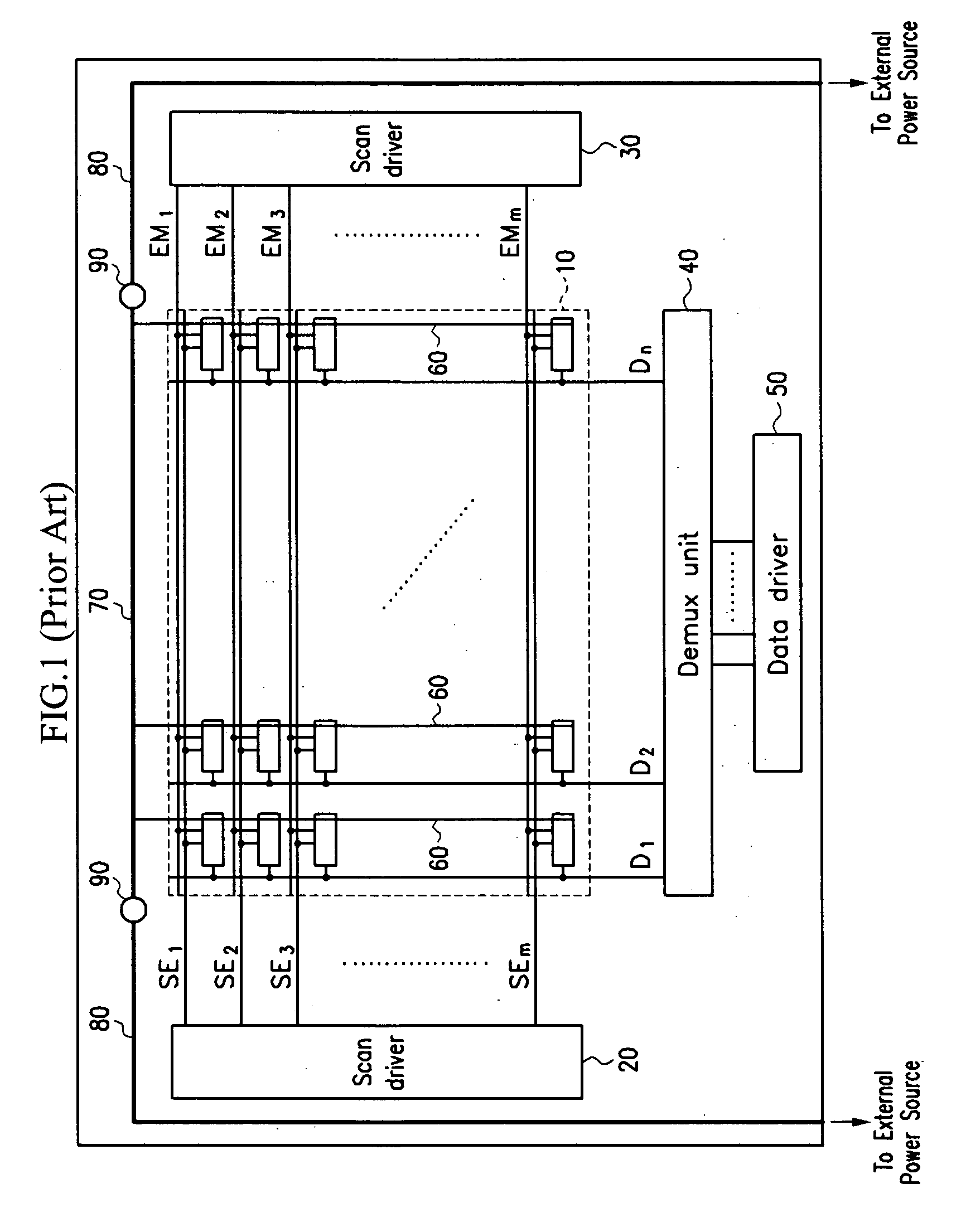
However, when a great voltage drop is generated, power consumption is increased due to a general need to enlarge the power supply voltage to obtain a sufficient margin of the saturation area.
Also, when sample / hold circuits are used for 1:N demultiplexing in the demultiplexer, it is generally required to sample the data current which corresponds to a data line during a 1 / N time of a particular horizontal period, shortening the sampling time, and hindering an appropriate sampling of the data current.

Method used


Image

  • Display device using demultiplexer and driving method thereof
  • Display device using demultiplexer and driving method thereof
  • Display device using demultiplexer and driving method thereof

Examples


second embodiment

[0107] In detail, the sample / hold circuit using transistor M1 having a threshold voltage which is higher, by a voltage of ∥ΔV1∥, than the absolute value of the threshold voltage of transistor M1 of the sample / hold circuit used for establishing precharge voltage range Ry in the second embodiment, that is, the absolute value ∥VTH∥ of the representative value of the threshold value has a gate voltage of transistor M1 which is lower than the case of the same current by the voltage of ∥ΔV1∥. Since the gate voltage of transistor M1 is a voltage charged in signal line X1, application of the same precharge voltage Vpre1 to the sample / hold circuit is substantially similar to applying the voltage of (Vpre1+∥ΔV1∥) obtained by adding the voltage of ∥ΔV1∥ to precharge voltage Vpre1 thereto as a precharge voltage. Therefore, when precharge voltage Vpre1 is included in precharge voltage range Ry, the precharge voltage of (Vpre1+∥ΔV1∥) may digress from precharge voltage range Ry in the sample / hold ...

third embodiment

[0109] Therefore, a voltage range which is lower than precharge voltage range Ry by ∥ΔV1∥ may be established to be the precharge voltage range when the absolute value of the threshold voltage is higher than the absolute value of the representative value by ∥ΔV1. Also, a voltage range which is higher than precharge voltage range Ry by ∥ΔV2∥ may be established to be the precharge voltage range when the absolute value of the threshold voltage is lower than the absolute value of the representative value by ∥ΔV2∥. Accordingly, when considering the deviation of the threshold voltages of sample / hold circuits, the difference of ∥ΔV3∥ between the absolute value of the representative value of the threshold value and the maximum value of the absolute value of the threshold value, and the difference of ∥ΔV4∥ between the absolute value of the representative value of the threshold value and the minimum value of the absolute value of the threshold, are applied to precharge voltage range Ry.

[0110]...

fourth embodiment

[0114] Therefore, precharge voltage Vpre can be given as Equation 3 in consideration of the voltage drop caused by the parasitic resistance of the power line in the

Vmin≦Vpre≦Vmax−∥ΔVDD∥   Equation 3 [0115] where Vmin is the minimum voltage within precharge voltage range Ry, and Vmax is the maximum voltage within precharge voltage range Ry.

[0116] Precharge voltage Vpre may be given as Equation 4 in consideration of the deviation of the threshold voltage of transistor M1 and the deviation of power supply voltage VDD1 described in the second and third embodiments.

Vmin+∥ΔV4∥≦Vpre≦Vmax−∥ΔV3∥−∥ΔVDD∥   Equation 4

[0117] The ranges of the precharge voltages have been described above. The respective sample / hold circuit units correspond to one of the red, green, and blue pixels since one sample / hold circuit unit corresponds to one data line. The voltage ranges of the precharge voltages may be differently established for the respective sample / hold circuits corresponding to the pixels of the ...


PUM


Abstract

Disclosed is a display device using a demultiplexer. The demultiplexer sequentially samples data currents that are time-divided and applied by a data driver, and holds them to a plurality of data lines. Since the demultiplexer is to sample the data currents corresponding to N data lines during a horizontal period when performing 1:N demultiplexing, the data current corresponding to one data line is to be sampled during a 1 / N horizontal period. According to one embodiment, a signal line coupled between the demultiplexer and the data driver is precharged with particular voltage before sampling the data current. The precharge voltage is sufficient to allow current transmitted to the signal line to be substantially sampled within a a given sampling time after the precharge voltage is applied.

Description

CROSS REFERENCE TO RELATED APPLICATION [0001] This application claims priority to and the benefit of Korean Patent Application No. 10-2003-0085078 filed on Nov. 27, 2003 in the Korean Intellectual Property Office, the entire content of which is incorporated herein by reference. BACKGROUND OF THE INVENTION [0002] (a) Field of the Invention [0003] The present invention relates to a display device using a demultiplexer. More specifically, the present invention relates to power wiring of a display device using a demultiplexer. [0004] (b) Description of the Related Art [0005] A display device generally requires a scan driver for driving scan lines and a data driver for driving data lines. The data driver has as many output terminals as it has data lines to convert digital data signals into analog signals and apply them to all of the data lines. In general, the data driver is configured with a plurality of integrated circuits (ICs). The plurality of ICs are used to drive all of the data l...

Claims


Application Information

Patent Timeline
IPC IPC(8): G09G3/20G09G3/30H01L51/50G09G3/32G09G3/36H04J3/06H05B33/14
CPCG09G3/325G09G3/3283G09G2300/0842G09G2320/0252G09G2310/0248G09G2310/0297G09G2300/0861G09G3/20
Inventor SHIN, DONG-YONG
Owner SAMSUNG DISPLAY CO LTD
Learn More