Optoelectronic device incorporating an interference filter

an optoelectronic device and interference filter technology, applied in the direction of lasers, laser output parameters control, laser construction details, etc., can solve the problems of high high loss of absorption loss of optical modes out of resonan

Inactive Publication Date: 2005-06-02
INNOLUME
View PDF20 Cites 127 Cited by
  • Summary
  • Abstract
  • Description
  • Claims
  • Application Information

AI Technical Summary

Benefits of technology

[0030] The interference filter of the present invention can be incorporated into a large variety of optoelectronic devices, including semiconductor diode lasers, optical amplifiers, resonant cavity photodetectors, wavelength-tunable lasers, amplifiers, and resonant photodetectors. The interference filter can also be incorporated into intensity-modulated diode lasers. Incorporation of the interference filter into an optoelectronic device results in wavelength-selective operation of the optoelectronic device.

Problems solved by technology

In some embodiments, the non-transparent element is an absorbing element, and the optical modes out of resonance exhibit high absorption losses.
In other embodiments, the non-transparent element is a scatterer, and the optical modes out of resonance exhibit high losses due to scattering.

Method used


Image

  • Optoelectronic device incorporating an interference filter
  • Optoelectronic device incorporating an interference filter
  • Optoelectronic device incorporating an interference filter

Examples


Embodiment Construction

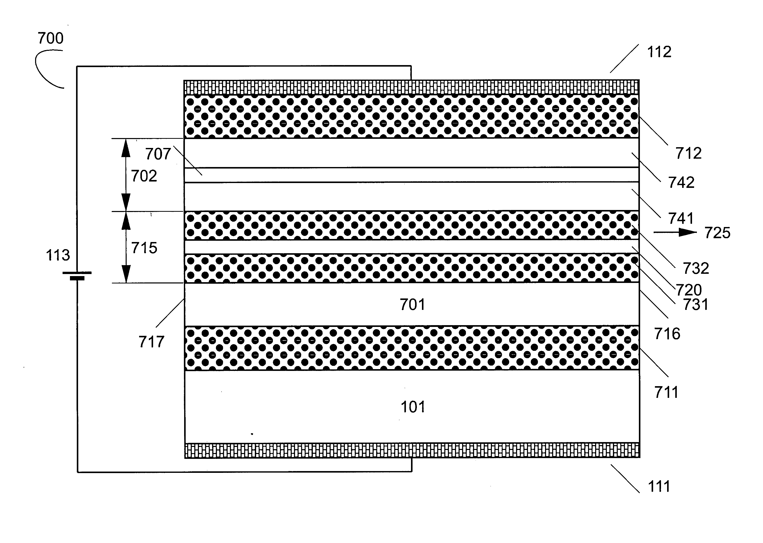
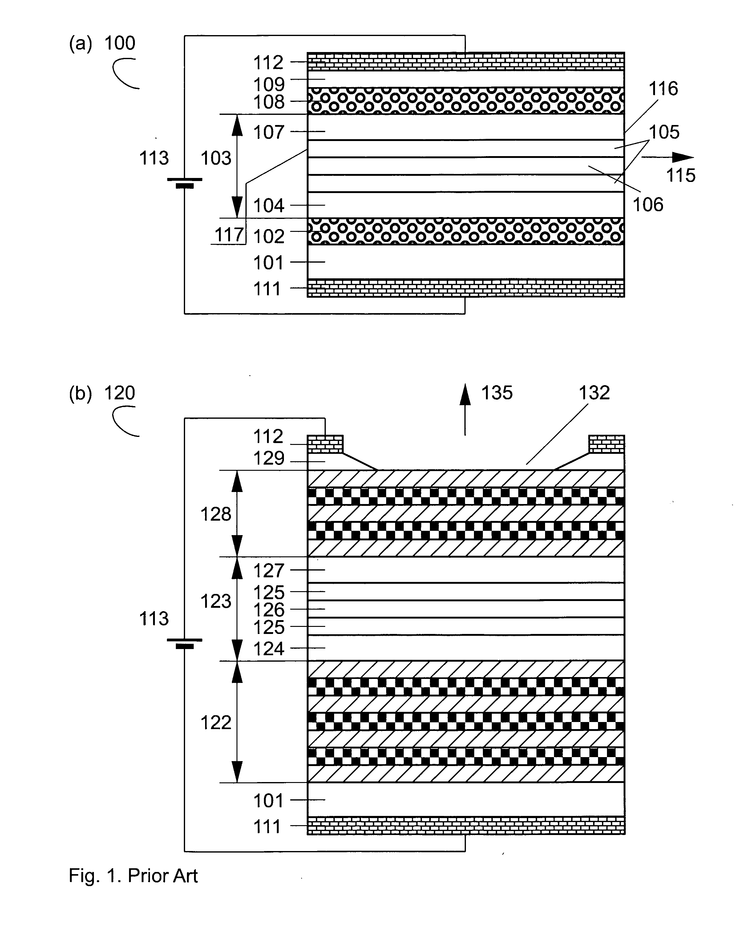
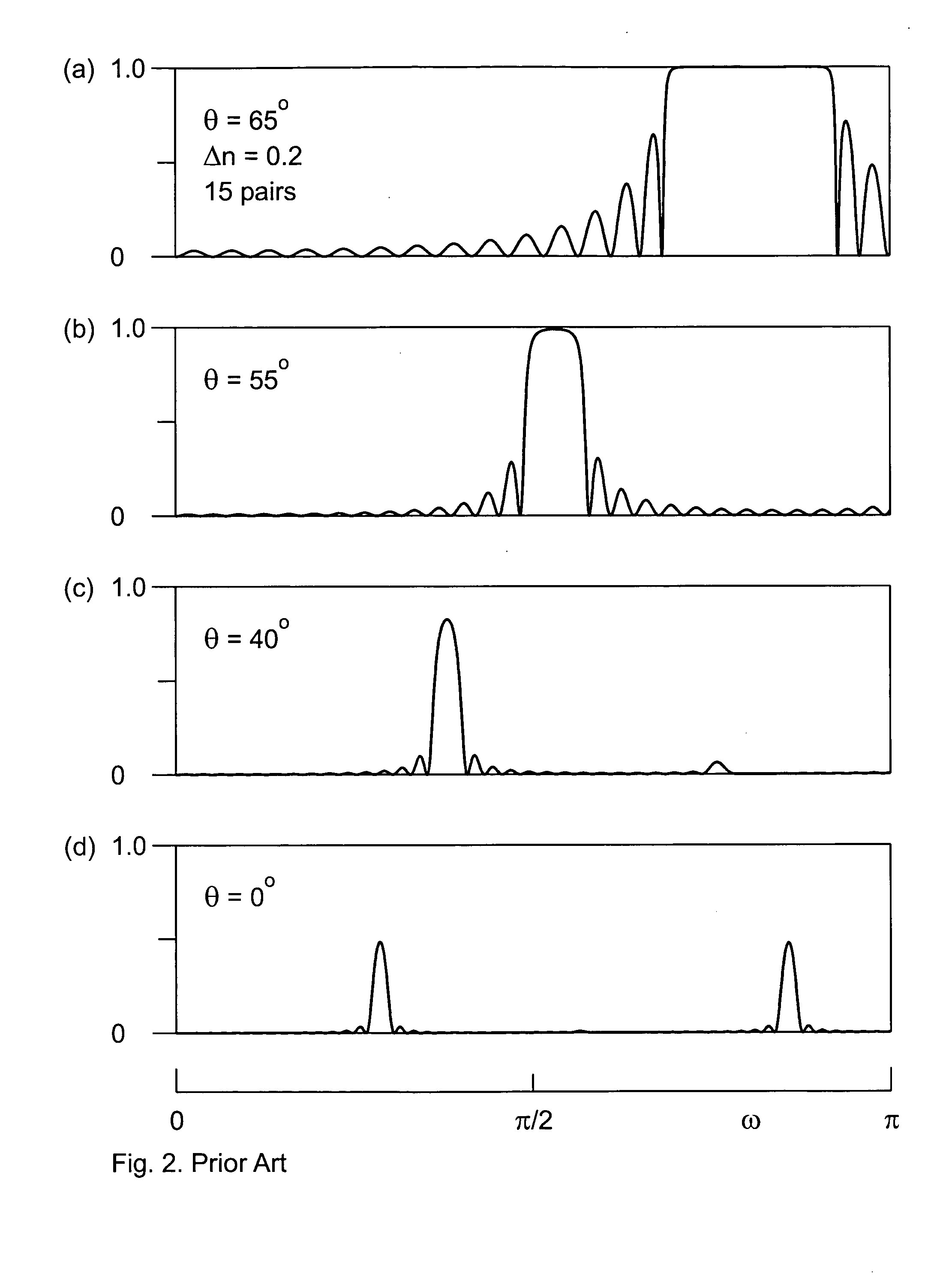
[0076] A way to overcome the shortcomings of optoelectronic devices, including, but not limited to, semiconductor diode lasers, switches, optical amplifiers, photodetectors, and light-emitting diodes, is related to different ways to construct a wavelength-selective light-emitting device. One of the ways to construct these devices is based on the fundamental physical properties of multilayered structures, i.e., on the laws of propagation, transmission, and reflection of electromagnetic waves at oblique incidence. FIG. 2 illustrates the reflectivity spectrum of a periodic multilayered structure for a few different tilt angles of the propagating TE electromagnetic wave, as described by A. Yariv and P. Yeh, in Optical Waves in Crystals. Propagation and Control of Laser Radiation, Wiley, 1984. Light comes from the medium with a refractive index n1=3.6, and the structure includes 15 periods. Each period further includes one layer of the Λ / 2 thickness having a low refractive index n2=3.4 a...


PUM


Abstract

A novel class of optoelectronic devices incorporate an interference filter. The filter includes at least two optical cavities. Each of the cavities localizes al least one optical mode. The optical modes localized at two cavities are at resonance only at one or at a few discrete selective wavelengths. At resonance, the optical eigenmodes contain one mode having a zero intensity at a node position between the two cavities, where this position shifts as a function of the wavelength. A non-transparent element, which is preferably an absorbing element, a scatterer, or a reflector, is placed between two cavities. At a discrete selective wavelength, when the node of the optical mode matches with the non-transparent element, the filter is transparent for light. At other wavelengths, the filter is not transparent for light. This allows for the construction of various optoelectronic devices showing a strongly wavelength-selective operation.

Description

REFERENCE TO RELATED APPLICATIONS [0001] This application claims an invention which was disclosed in Provisional Application No. 60 / 526,409, filed Dec. 1, 2003, entitled “TILTED CAVITY SEMICONDUCTOR LIGHT-EMITTING DEVICE AND METHOD OF MAKING SAME” and Provisional Application No. 60 / 577,537, filed Jun. 7, 2004, entitled “ELECTROOPTICALLY WAVELENGTH-TUNABLE RESONANT CAVITY OPTOELECTRONIC DEVICE FOR HIGH-SPEED DATA TRANSFER”. The benefit under 35 USC §119(e) of the provisional applications is hereby claimed, and the aforementioned applications are hereby incorporated herein by reference.BACKGROUND OF THE INVENTION [0002] 1. Field of the Invention [0003] The invention pertains to the field of optoelectronic devices. More particularly, the invention pertains to semiconductor edge-emitting and surface-emitting lasers, optical amplifiers, photodetectors, wavelength-tunable vertical cavity lasers, optical filters, optical switches, wavelength-tunable tilted cavity lasers, wavelength-tunable...

Claims


Application Information

Patent Timeline
Patent Type & Authority Applications(United States)
IPC IPC(8): G02B5/28H01J61/40H01L31/0216H01L33/10H01S5/026H01S5/042H01S5/06H01S5/10H01S5/183H01S5/20H01S5/40
CPCG02B5/285H01S2301/18H01L31/02165H01L33/105H01S5/026H01S5/0425H01S5/0654H01S5/0656H01S5/1021H01S5/1032H01S5/18302H01S5/18311H01S5/1833H01S5/2004H01S5/2022H01S5/2027H01S5/4043G02B5/288
Inventor SHCHUKIN, VITALYLEDENTSOV, NIKOLAI
Owner INNOLUME
Why Eureka
Try Eureka