
Control of phosphorus profile by carbon in-situ doping for high performance vertical PNP transistor

a technology of phosphorus profile and carbon in-situ doping, which is applied in the direction of transistors, semiconductor devices, electrical equipment, etc., can solve the problems of unavoidably broadening the base layer, undesirable large process fluctuation, and no narrow base profiles obtainabl

Inactive Publication Date: 2005-06-02
TEXAS INSTR INC
View PDF7 Cites 0 Cited by
  • Summary
  • Abstract
  • Description
  • Claims
  • Application Information

AI Technical Summary

Benefits of technology

[0005] The present invention provides a method of producing a vertical bipolar PNP transistor comprising the steps of incorporating carbon in the base layer only in the vicinity of a junction zone between the collector layer and the base layer, doping said base layer with phosphorous and subjecting the doped base layer to a thermal treatment such that phosphorous is allowed to diffuse out from the surface area of the base layer and towards said junction zone and phosphorous is prevented from diffusing towards the junction zone by the presence of carbon.
[0008] The high phosphorous concentration near the surface caused by low energy implant can, on the one hand, diffuse out quickly and, on the other hand, diffuse towards the junction zone, thus increasing the concentration of phosphorous in the base layer.

Problems solved by technology

One commonly used N-dopant for the base layer of PNP transistors is phosphorous, but with its high diffusivity in silicon there are no narrow base profiles obtainable.
In fact, phosphorous diffuses in a following annealing step into the underlying layer, thus unavoidably broadening the base layer.
This leads to an undesirable large process fluctuation.
This high dopant concentration may later lead to emitter-base junction leakages at the emitter periphery.
All considered, there is a clear dead end to improve PNP transistor performance by only modifying the arsenic implant condition.

Method used


Image

  • Control of phosphorus profile by carbon in-situ doping for high performance vertical PNP transistor
  • Control of phosphorus profile by carbon in-situ doping for high performance vertical PNP transistor

Examples


Embodiment Construction

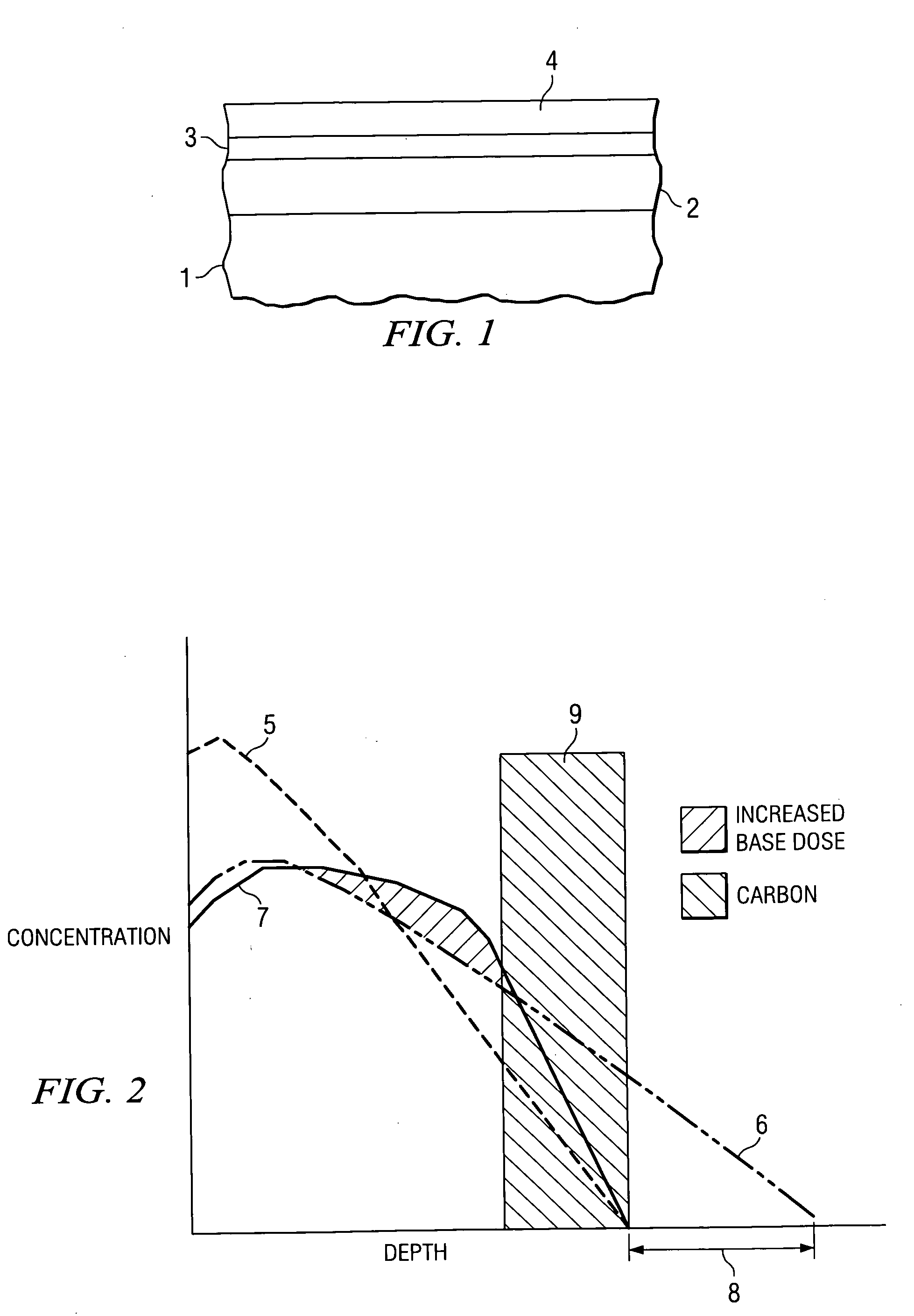
[0014]FIG. 1 shows schematically the superposed layers of a vertical bipolar PNP transistor, where 1 is a substrate, 2 is a P-doped collector layer, 3 is an N-doped base layer and 4 is a P-doped emitter layer. These layers are conventionally grown epitaxially on the substrate. In the case of a high frequency transistor, the thickness of the base layer, the dopant concentration and the dopant profile are essential for high speed.

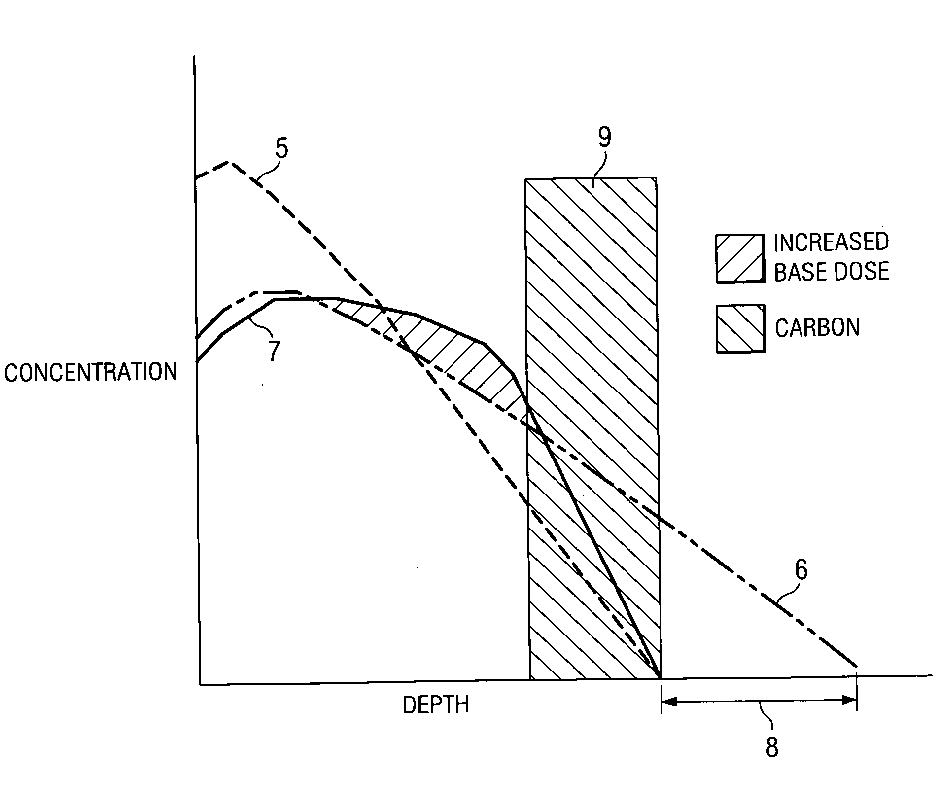
[0015]FIG. 2 shows doping profiles of a base layer of a vertical PNP transistor. In FIG. 2, zero depth corresponds to the interface between the emitter and base layers. The dashed line 5 in the graph shows the concentration of phosphorous as implanted. The dashed line 6 shows the phosphorous profile that would result after an annealing step, if no carbon were present in the base layer. A shaded rectangle 9 indicates a zone of a depth in the base layer where carbon is present. Line 7 in FIG. 2 shows the phosphorous concentration with the presence of carbon in...


PUM


Abstract

A method of producing a vertical bipolar PNP transistor is disclosed. The phosphorous profile in the base layer is controlled. Carbon that is incorporated in the base layer in the vicinity of the base-collector junction suppresses the diffusion of phosphorous deeper than implanted in a subsequent thermal step. PNP transistors with a narrow phosphorous-doped base can thus be manufactured with a cut-off frequency increased from 23 GHz to 30 GHz.

Description

FIELD OF THE INVENTION [0001] The present invention relates to a method of producing a vertical PNP transistor from a semiconductor material, comprising the steps of providing a collector layer, forming a base layer on said collector layer, doping said base layer with phosphorous and forming an emitter layer on top of said base layer. The present invention further relates to a vertical PNP transistor produced by this method. BACKGROUND OF THE INVENTION [0002] Integrated circuits often include vertical PNP transistors that are transistors with superposed layers. One of the general requirements for high performance analog circuits is the bipolar high speed and low base resistance. In order to meet both requirements, the base profile should be narrow with a high dopant concentration. [0003] One commonly used N-dopant for the base layer of PNP transistors is phosphorous, but with its high diffusivity in silicon there are no narrow base profiles obtainable. In fact, phosphorous diffuses ...

Claims


Application Information

Patent Timeline
Patent Type & Authority Applications(United States)
IPC IPC(8): H01L21/331H01L29/10H01L29/73H01L29/732H01L29/737
CPCH01L29/1004H01L29/66242H01L29/7378H01L29/732H01L29/66287
Inventor YASUDA, HIROSHIEL-KAREH, BADIHBALSTER, SCOTTSCHIEKOFER, MANFRED
Owner TEXAS INSTR INC
Learn More