Thrust pad assembly for ECP system

a thrust pad and assembly technology, applied in the field of electrochemical plating systems, can solve the problems of device failure or burn-in, complex interconnection of components in the circuit, and subjected to precise dimensional control, so as to reduce the quantity of metal electroplated onto the edge region, reduce the ohmic contact, and reduce the effect of pressur

Inactive Publication Date: 2005-06-09
TAIWAN SEMICON MFG CO LTD
View PDF6 Cites 4 Cited by
  • Summary
  • Abstract
  • Description
  • Claims
  • Application Information

AI Technical Summary

Benefits of technology

[0021] In accordance with these and other objects and advantages, the present invention is generally directed to a new and improved thrust pad assembly which is capable of reducing the quantity of metal electroplated onto the edge region of a substrate to eliminate or reduce the need for edge bevel cleaning or removal of excess metal from the substrate after the electroplating process. The thrust pad assembly typically includes an air platen through which air is applied at variable pressures to the central and edge regions, respectively, of a thrust pad. The thrust pad applies pressure to a contact ring connected to an electroplating voltage source. The contact ring applies relatively less pressure to the edge region than to the central region of the substrate, thereby reducing the ohmic contact between the contact ring and the edge region of the substrate. Therefore, excess electroplating of the metal onto the edge regions of the substrate is eliminated or substantially reduced.

Problems solved by technology

Due to the ever-decreasing size of semiconductor components and the ever-increasing density of integrated circuits on a wafer, the complexity of interconnecting the components in the circuits requires that the fabrication processes used to define the metal conductor line interconnect patterns be subjected to precise dimensional control.
These voids or open circuits may cause device failure or burn-in.
However, such edge bevel cleaning of wafers required after electroplating is a common source of process flow bottlenecking and hinders orderly and efficient flow of the electroplating process sequence.

Method used


Image

  • Thrust pad assembly for ECP system
  • Thrust pad assembly for ECP system
  • Thrust pad assembly for ECP system

Examples


Embodiment Construction

[0030] The present invention has particularly beneficial utility in the electroplating of copper or other metals onto a semiconductor wafer substrate in the fabrication of integrated circuits on the substrate. However, the invention is not so limited in application, and while references may be made to such semiconductor wafer substrate and integrated circuits, the invention may be more generally applicable to electroplating metals on substrates in a variety of industrial applications.

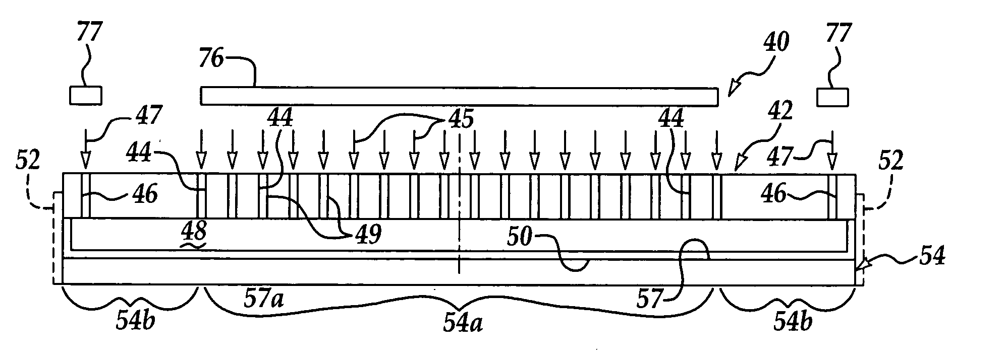
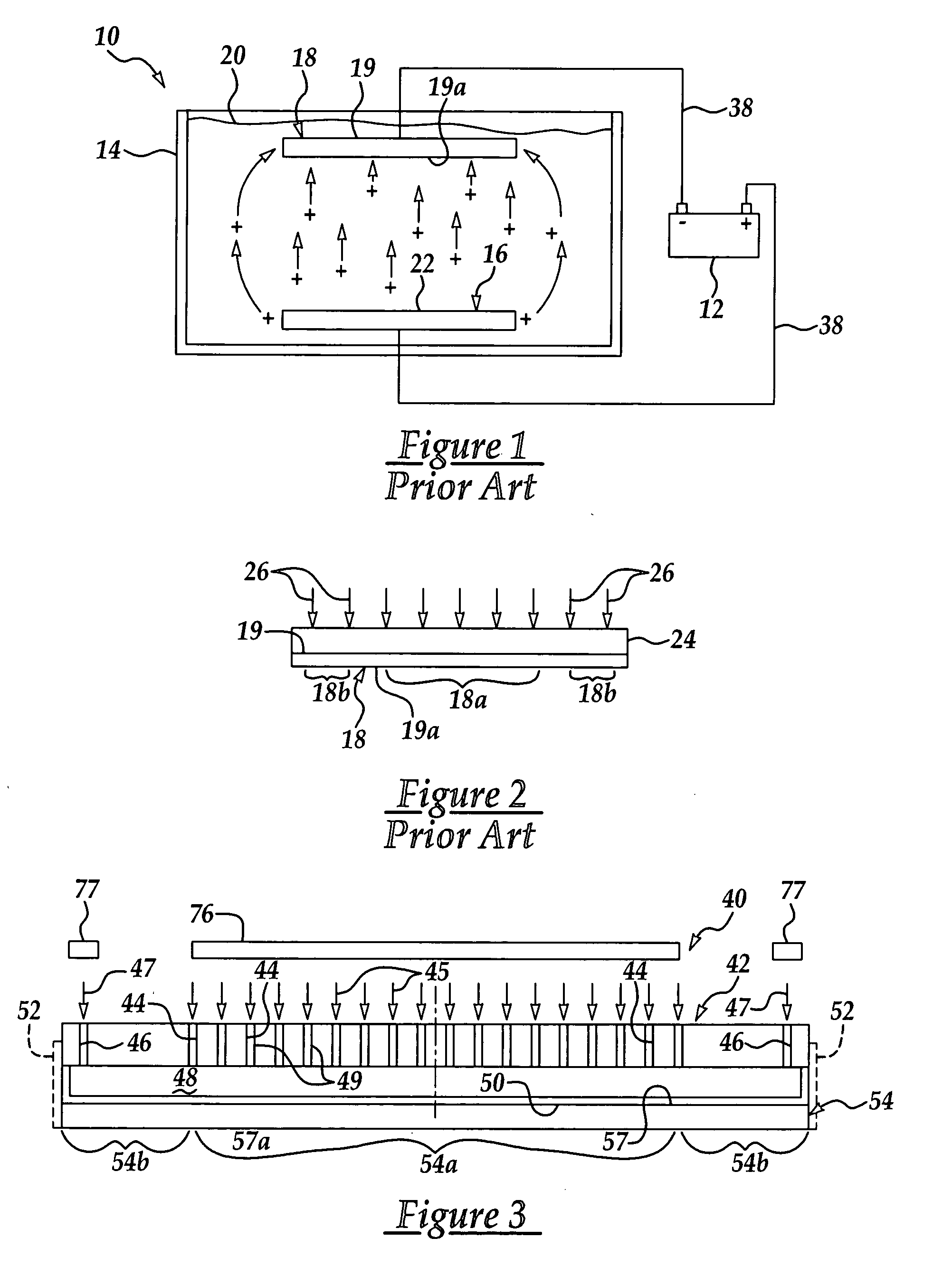
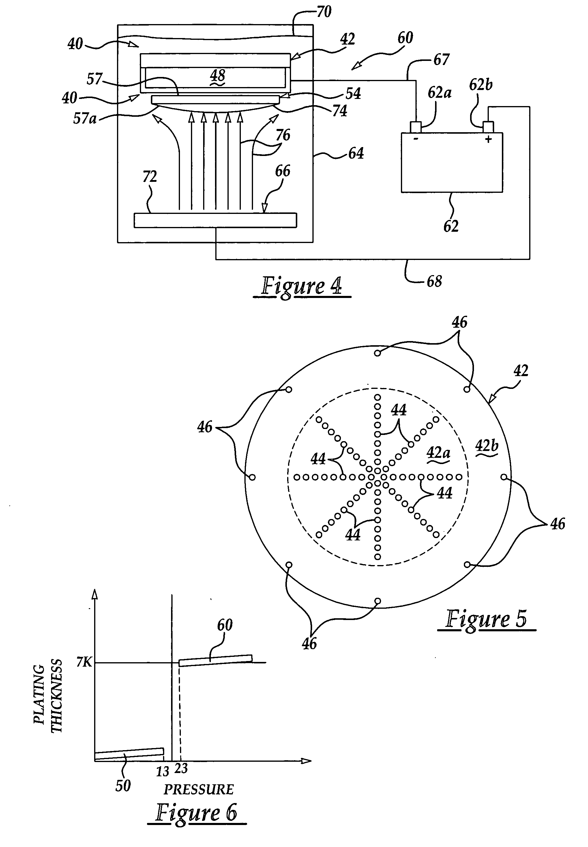
[0031] The present invention is generally directed to a new and improved thrust pad assembly which is suitable for preventing deposition of excess quantities of metal onto the edge or peripheral region of a substrate as copper or other metal is electroplated onto the substrate in the fabrication of semiconductor integrated circuits on the substrate. The thrust pad assembly eliminates the need for edge bevel cleaning or removal of excess metal from the edge region of the substrate after the electroplati...


PUM

PropertyMeasurementUnit
peripheral pressureaaaaaaaaaa
air pressureaaaaaaaaaa
thicknessaaaaaaaaaa

Abstract

A thrust pad assembly which is capable of reducing the quantity of metal electroplated onto the edge region of a substrate to eliminate or reduce the need for edge bevel cleaning or removal of excess metal from the substrate after the electroplating process. The thrust pad assembly includes an air platen through which air is applied at variable pressures to the central and edge regions, respectively, of a thrust pad. The thrust pad applies pressure to a contact ring connected to an electroplating voltage source. The contact ring applies relatively less pressure to the edge region than to the central region of the substrate, thereby reducing the ohmic contact.

Description

FIELD OF THE INVENTION [0001] The present invention relates to electrochemical plating systems used in the deposition of metal layers on semiconductor wafer substrates in the fabrication of semiconductor integrated circuits. More particularly, the present invention relates to an electrochemical plating system having a thrust pad assembly which reduces the quantity of metal electroplated on the edge regions of a cathode / wafer by the application of variable pressure to the center and edge regions of the wafer. BACKGROUND OF THE INVENTION [0002] In the fabrication of semiconductor integrated circuits, metal conductor lines are used to interconnect the multiple components in device circuits on a semiconductor wafer. A general process used in the deposition of metal conductor line patterns on semiconductor wafers includes deposition of a conducting layer on the silicon wafer substrate; formation of a photoresist or other mask such as titanium oxide or silicon oxide, in the form of the de...

Claims


Application Information

Patent Timeline
Patent Type & Authority Applications(United States)
IPC IPC(8): C25D5/02C25D5/06C25D7/12C25D17/14H01L21/288
CPCC25D5/06C25D17/001H01L21/2885C25D17/14
Inventor TSAO, JUNG-CHIHCHEN, KEI-WEILIU, CHI-WENLIN, SHI-CHICHUANG, RAY
Owner TAIWAN SEMICON MFG CO LTD
Why Eureka
Try Eureka