

Surface structures for halo reduction in electron bombarded devices
- Summary
- Abstract
- Description
- Claims
- Application Information
AI Technical Summary
Benefits of technology
Problems solved by technology
Method used
Image

Examples
Embodiment Construction
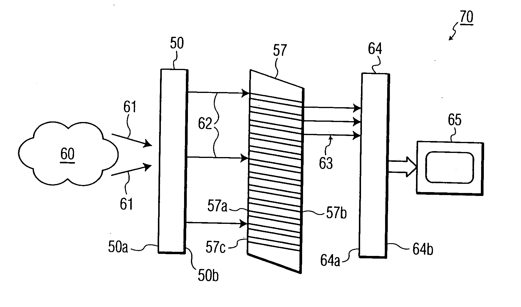
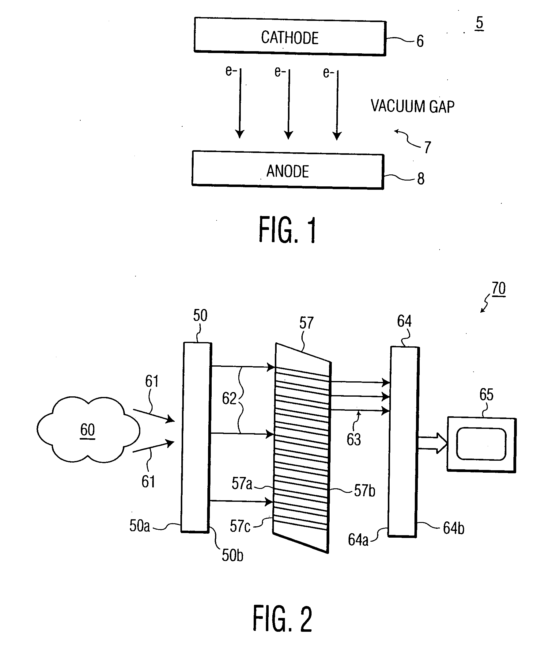
[0030] As will be explained, the present invention reduces backscattering of electrons, reduces the halo phenomenon and increases gain of an electron bombarded device, by providing a textured surface to the electron collection surface of the device.
[0031] Referring to FIG. 1, there is shown an electron bombarded device, generally designated as 5. The device includes cathode 6 and anode 8 which are spatially separated by vacuum gap 7. The anode serves as the electron collection point.
[0032] It will be appreciated that electrons are emitted from cathode 6 into vacuum gap 7 by either a negative electron affinity surface (NEA), positive electron affinity surface (PEA), thermionic emission, or field emission. An electric field (not shown) between the cathode and anode accelerates the electrons towards anode 8. Extra electrodes (not shown) with various potentials may also be placed between the cathode and anode to focus the electrons. These electrodes do not change the overall landing p...
PUM
 Abstract
Description
Claims
Application Information