Light-emitting device comprising led chip and method for manufacturing this device

Inactive Publication Date: 2005-06-09
ROHM CO LTD
View PDF5 Cites 81 Cited by
  • Summary
  • Abstract
  • Description
  • Claims
  • Application Information

AI Technical Summary

Benefits of technology

[0023] With such a method, unlike the prior art technique, a light emitting device having the above-des

Problems solved by technology

Further, the configuration cannot be made generally uniform with respect to a plurality of lens members 7, and the variation of the configuration of the lens members i

Method used


Image

  • Light-emitting device comprising led chip and method for manufacturing this device
  • Light-emitting device comprising led chip and method for manufacturing this device
  • Light-emitting device comprising led chip and method for manufacturing this device

Examples


first embodiment

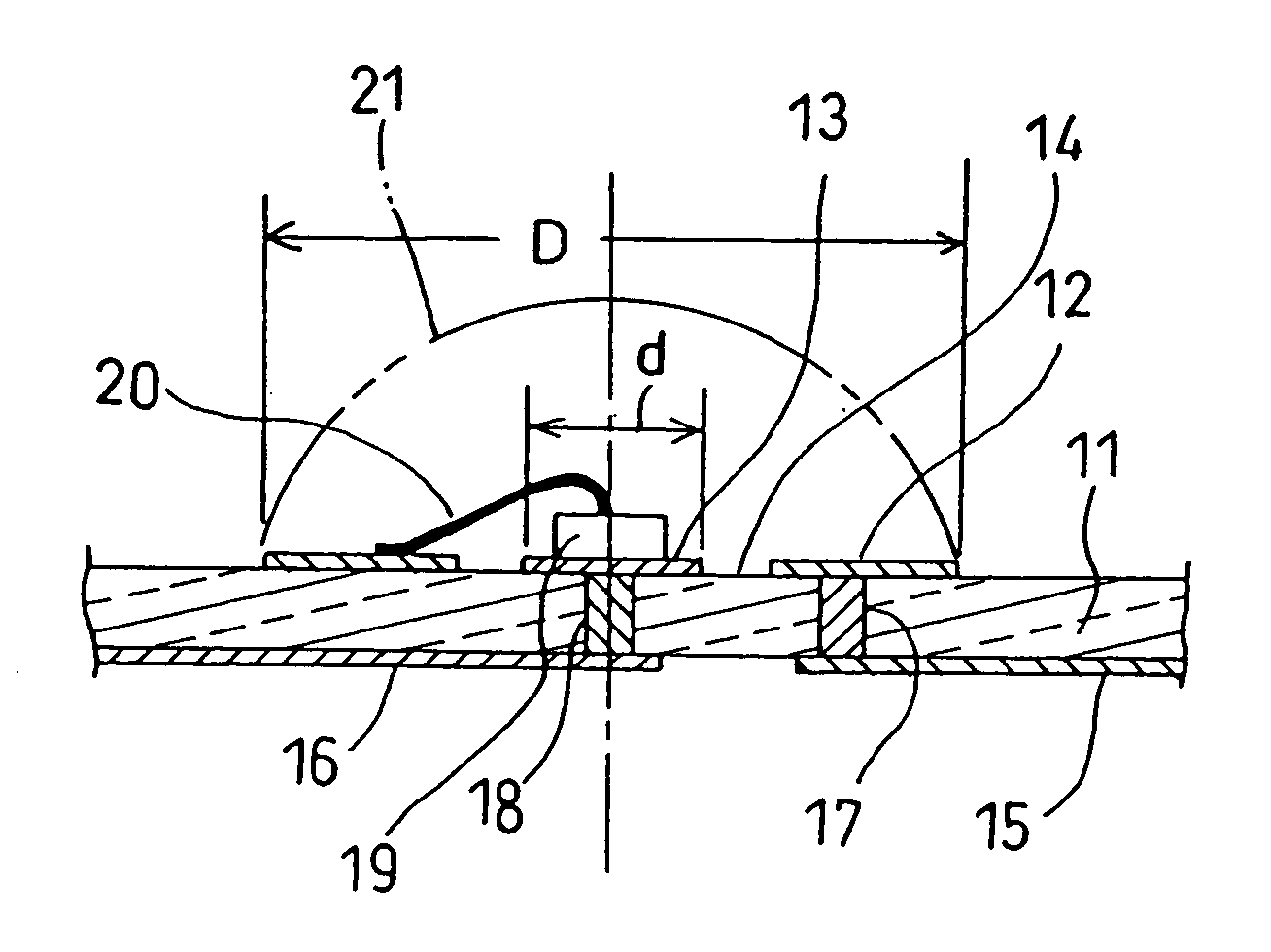
[0038]FIGS. 1 and 2 show the present invention. In this embodiment, a single LED chip is utilized.

[0039] Designated by the reference sign 11 in these figures is a wiring board made of an insulating material such as glass-fiber-reinforced epoxy resin (glass fibers hardened with an epoxy resin). On the upper surface of the wiring board 11 are formed a first patterned electrode 12 and a second patterned electrode 13, which are made of a metal film comprising a copper foil and a gold plating layer formed thereon via an underlying nickel plating layer, for example.

[0040] The first patterned electrode 12 is circular with a diameter D. The first patterned electrode 12 has a cutout 14 at the center thereof. The second patterned electrode 13 is circular with a smaller diameter d and arranged in the cutout 14 of the first patterned electrode 12 while being spaced from the first patterned electrode 12 like an island.

[0041] On the lower surface of the wiring board 11 are formed a power supply...

third embodiment

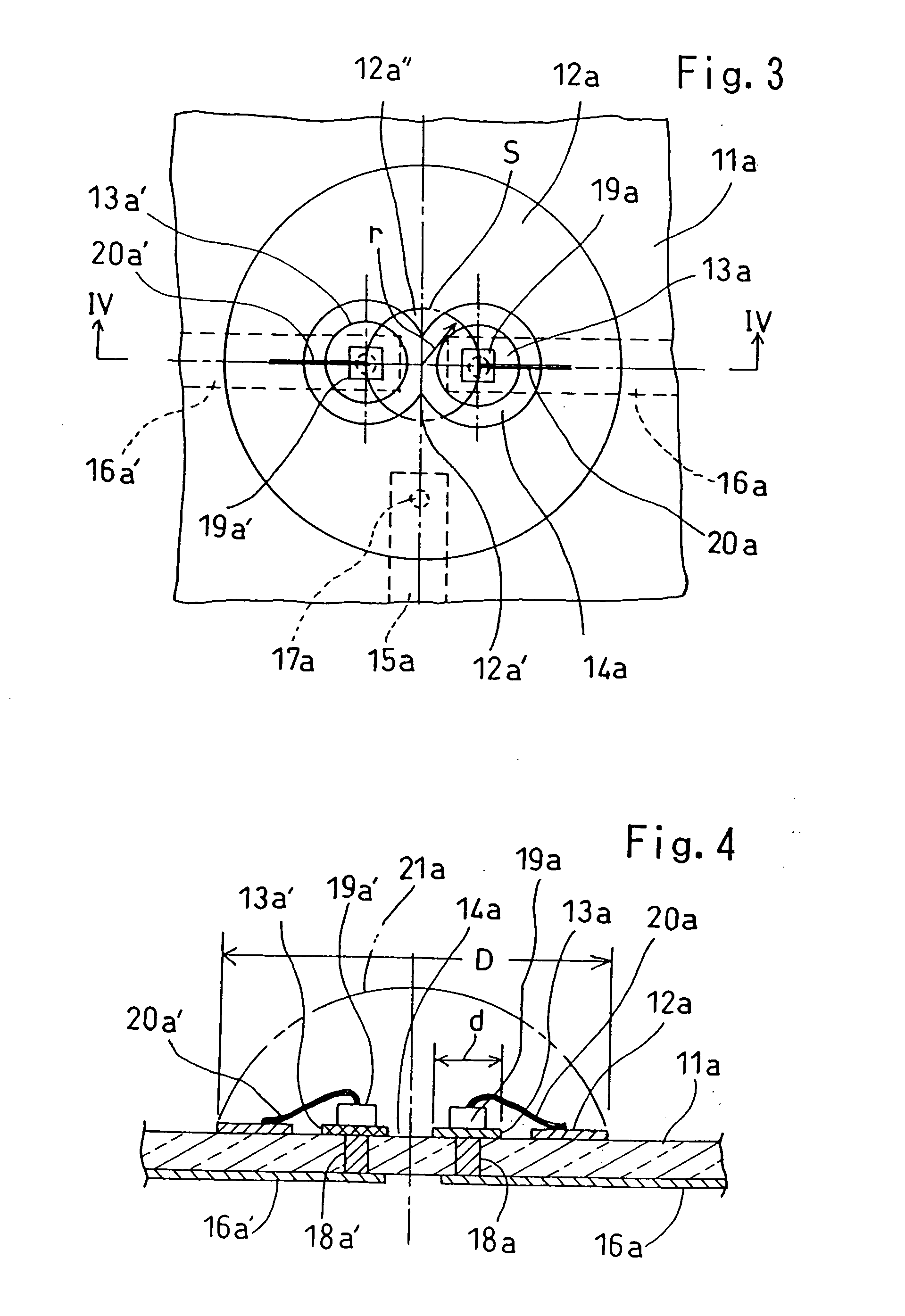
[0055]FIGS. 5 and 6 show the present invention.

[0056] In the third embodiment, three LED chips, i.e., an LED chip 19b for emitting red light, an LED chip 19b′ for emitting green light, and an LED chip 19b″ for emitting blue light are utilized.

[0057] Designated by the reference sign 11b in these figures is a wiring board made of an insulating material. On the upper surface of the wiring board 11b, a first patterned electrode 12b and three second patterned electrode 13b, 13b′, 13b″ are formed, which are made of a metal film similarly to those of the first and the second embodiments.

[0058] The first patterned electrode 12b is circular with a diameter D. The first patterned electrode 12b has a cutout 14b at the center thereof. Each of the three second patterned electrodes 13b, 13b′, 13b″ is circular with a smaller diameter d. The three second patterned electrodes 13b, 13b′, 13b″ are arranged, like islands, in the cutout 14b of the first patterned electrode 12b while being equally spac...

fourth embodiment

[0065]FIGS. 7, 8 and 9 show a

[0066] In the fourth embodiment, a number of light emitting devices 22 according to the third embodiment are arranged in a matrix of rows and columns on a single common wiring board 23, thereby providing a panel for displaying letters or images in full color utilizing three primary colors of light.

[0067] In the fourth embodiment, a conductor pattern 24 is formed on the entire upper surface of the common wiring board 23 except the portions formed with the first circular patterned electrodes 12b, with a ring-like gap 25 formed between the conductor pattern 24 and each of the first patterned electrodes 12b. The conductor pattern 24 is electrically connected to the first patterned electrode 12b of each light emitting device 22 via a power supply wiring pattern 26 formed on the lower surface of the common wiring board 23 and through holes 27, 28, 29.

[0068] As indicated by double-dashed lines, the obverse surface of the conductor pattern 24 is covered with a...


PUM


Abstract

A light emitting device includes a first patterned electrode 12 and a second patterned electrode 13 both of which are formed on a wiring board 11, an LED chip 19 mounted on the second patterned electrode 13, a metal wire 20 electrically connecting the LED chip 19 and the first patterned electrode 12 to each other, and a lens member 21 made of a transparent synthetic resin for packaging the LED chip 19 and the metal wire 20. The first patterned electrode 12 is circular and formed with a cutout 14 at the center thereof. The second patterned electrode 13 is arranged in the cutout 14. With this arrangement, the lens member 21 can be formed into a predetermined configuration, while the reflection of light by the patterned electrodes can be ensured.

Description

BACKGROUND OF THE INVENTION [0001] 1. Field of the Invention [0002] The present invention relates to a light emitting device including an LED chip mounted on e.g. a printed wiring board and packaged in a lens member made of a synthetic resin, while also relating to a method of making such a device. [0003] 2. Description of the Related Arts [0004] A typical light emitting device of the above-described type includes a pair of first patterned electrode and second patterned electrode formed on an upper surface of a wiring board. On the upper surface of the second patterned electrode is mounted an LED chip, which is electrically connected to the first patterned electrode by wire bonding using a thin metal wire. A lens member made of a transparent synthetic resin is formed on the upper surface of the wiring board at the portion where the LED chip is mounted to package the LED chip and the metal wire. [0005]FIGS. 10 and 11 show a structure disclosed in JP-A 4-28269 as a prior art device. S...

Claims


Application Information

Patent Timeline
IPC IPC(8): H01L33/62H01L21/316H01L25/075H01L33/56H01L33/58H01L33/60
CPCH01L21/02126H01L2924/12041H01L21/02203H01L21/02263H01L21/02282H01L21/02337H01L21/31604H01L21/31608H01L21/31695H01L25/0753H01L33/486H01L33/52H01L33/62H01L2224/48091H01L2224/48227H01L21/02197H01L2924/00014
Inventor ITAI, JUNICHIISHIHARA, TAKAYUKIKITAMURA, TAKESHI
Owner ROHM CO LTD
Why Eureka
Try Eureka