

One-drop fill spacerless process for liquid crystal cell on a silicon backplane or microdisplays
- Summary
- Abstract
- Description
- Claims
- Application Information
AI Technical Summary
Benefits of technology
Problems solved by technology
Method used
Image

Examples
Embodiment Construction
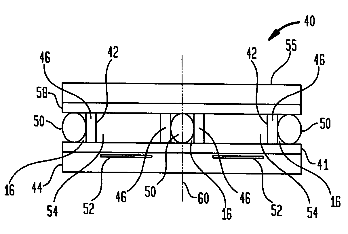
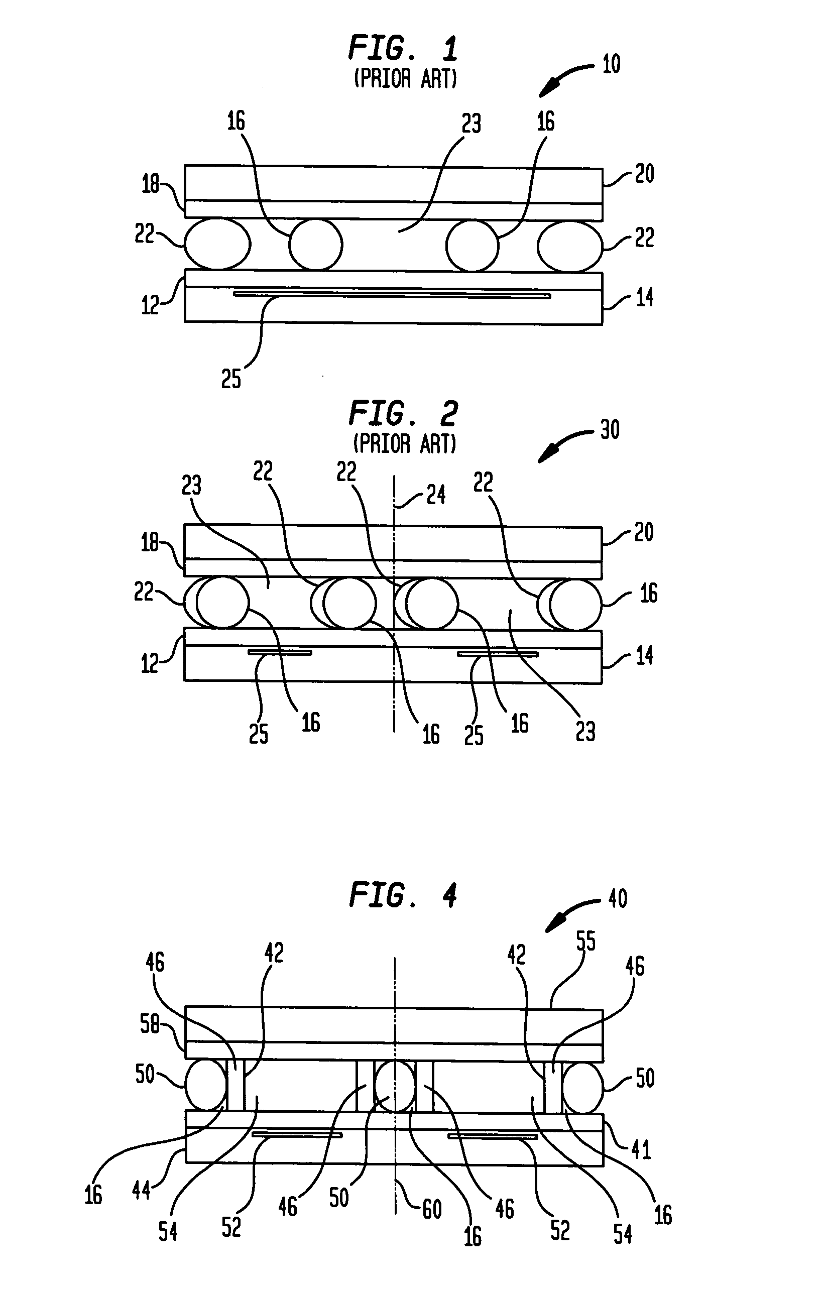
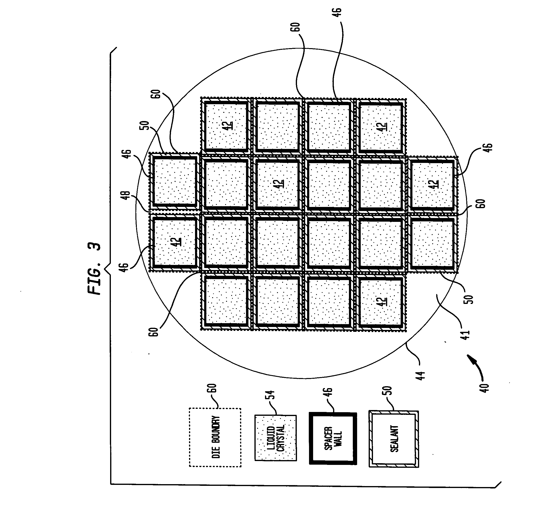
[0018] Referring now in more specific detail to the drawings, as shown in the prior art representation of FIG. 1, there is illustrated a single liquid crystal display cell assembly 10 showing the manufacture thereof pursuant to the prior art. In this case, an alignment layer 12 is positioned on a TFT substrate or silicon die 14, and a sealant 22 is applied to the perimeter of the single cell, the latter of which is equipped with spacer balls or posts 16. An upper alignment layer 18 is then positioned on the spacer balls or posts 16 and a glass window layer 20 positioned thereon. During assembly, air is provided and then liquid crystal 23 is filled into the cell, producing active liquid crystal display area 25, whereupon curing of sealant 22 is effected.
[0019] As illustrated in FIG. 2 of the drawings, this illustrates a prior art liquid crystal cell-forming method, in which the components are analogous to those of FIG. 1, and identified by the same reference numerals. However, in th...
PUM
 Abstract
Description
Claims
Application Information