Optical element, lithographic apparatus including such optical element and device manufacturing method, and device manufactured thereby

Inactive Publication Date: 2005-06-09
ASML NETHERLANDS BV
View PDF12 Cites 39 Cited by
  • Summary
  • Abstract
  • Description
  • Claims
  • Application Information

AI Technical Summary

Benefits of technology

[0016] In still another embodiment, the transmissive top layer includes at least Ru. Ru is relatively more stable to oxidation than, for example, Si. In this way, subwavelength roughness is introduced by a relatively stable transmissive top layer including the structure. Such transmissive top layer also provides protection of the optical element, for example to oxidation. In another embodiment, the transmissive top layer and the structure include Ru. In U.S. Pat. No. 6,678,037, the Ru layer may only provide protect

Problems solved by technology

These unwanted frequencies will propagate and cause heating problems in the illumination and projection systems and cause unwanted exposure of the resist if not blocked; although the multilayer mirrors of the illumination and projection systems are designed for reflection of the desired wavelength, e.g. 13 nm, they are optically flat and have quite high reflectivities at IR, visible and UV wavelengt

Method used


Image

  • Optical element, lithographic apparatus including such optical element and device manufacturing method, and device manufactured thereby
  • Optical element, lithographic apparatus including such optical element and device manufacturing method, and device manufactured thereby
  • Optical element, lithographic apparatus including such optical element and device manufacturing method, and device manufactured thereby

Examples


Embodiment Construction

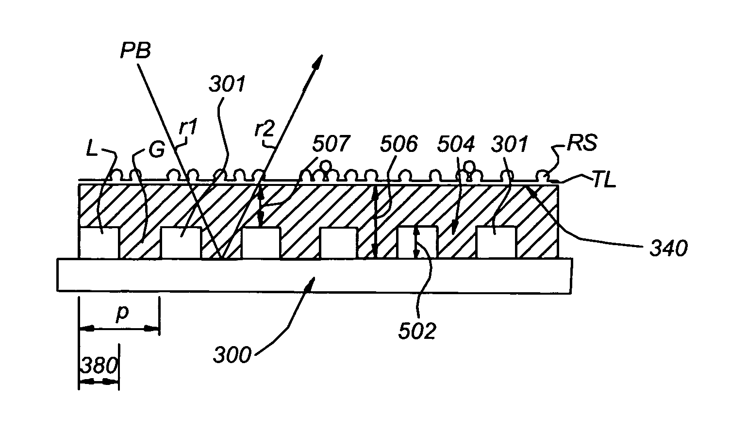
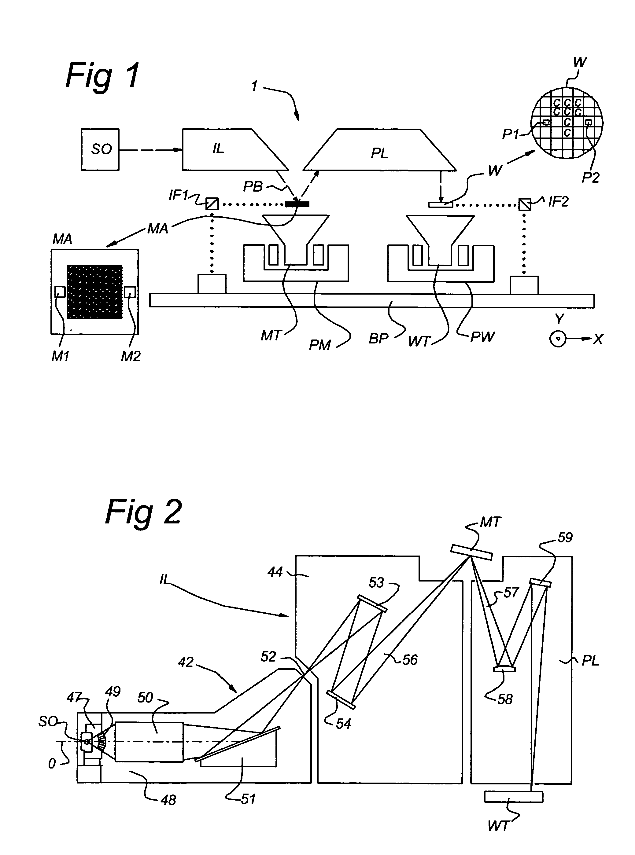
[0072]FIG. 1 schematically depicts a lithographic apparatus 1 according to the present invention. The apparatus 1 includes a base plate BP. An illumination system (illuminator) IL is configured to provide a beam of radiation PB of radiation (e.g. UV or EUV radiation). A first support (e.g. a mask table) MT is configured to support a patterning device (e.g. a mask) MA and is connected to a first positioning device PM that accurately positions the patterning device with respect to a projection system PL. A substrate table (e.g. a wafer table) WT is configured to hold a substrate (e.g. a resist-coated wafer) W and is connected to second positioning device PW that accurately positions the substrate with respect to the projection system PL. The projection system (e.g. a reflective projection lens) PL is configured to image a pattern imparted to the beam of radiation PB by patterning device MA onto a target portion C (e.g. including one or more dies) of the substrate W.

[0073] As here dep...


PUM

PropertyMeasurementUnit
Nanoscale particle sizeaaaaaaaaaa
Wavelengthaaaaaaaaaa
Surface roughnessaaaaaaaaaa

Abstract

An optical element includes a top layer which is transmissive for EUV radiation with wavelength λ in the range of 5-20 nm, and a structure of the top layer is a structure having an rms roughness value equal to or larger than λ/10 for spatial periods equal to or smaller than λ/2. The structure promotes transmission through the top layer to the optical element.

Description

[0001] This application claims priority to European Patent Application 03078495.3, filed Nov. 6, 2003, the contents of which are herein incorporated by reference. BACKGROUND OF THE INVENTION [0002] 1. Field of the Invention [0003] The present invention relates to an optical element, a lithographic apparatus including such optical element, a device manufacturing method and a device manufactured thereby. [0004] 2. Description of the Related Art [0005] A lithographic apparatus is a machine that applies a desired pattern onto a target portion of a substrate. Lithographic apparatus can be used, for example, in the manufacture of integrated circuits (ICs). In that circumstance, a patterning device, such as a mask, may be used to generate a circuit pattern corresponding to an individual layer of the IC, and this pattern can be imaged onto a target portion (e.g. including part of one or several dies) on a substrate (e.g. a silicon wafer) that has a layer of radiation-sensitive material (res...

Claims


Application Information

Patent Timeline
IPC IPC(8): G02B1/11G02B5/02G02B5/00G02B5/08G03F7/20H01L21/027
CPCG02B1/11G02B5/00Y10T428/24355G03F7/70191G03F7/70233
Inventor BAKKER, LEVINUS
Owner ASML NETHERLANDS BV
Why Eureka
Try Eureka