Semiconductor integrated circuit device

a technology of integrated circuits and semiconductors, applied in the direction of emergency protective circuit arrangements, etc., can solve the problems of high-integrated semiconductor ic devices, large area, and increased current consumption, so as to prevent esd breakdown in matching circuits. , the effect of ensuring the stability

Inactive Publication Date: 2005-06-09
RENESAS ELECTRONICS CORP
View PDF9 Cites 13 Cited by
  • Summary
  • Abstract
  • Description
  • Claims
  • Application Information

AI Technical Summary

Benefits of technology

[0008] An object of the present invention is to provide a semiconductor IC device for reliably preventing ESD breakdown in a matching circuit including resistance elements and transistors.

Problems solved by technology

By decreasing the ON-resistance of the MOS transistors M31 to M38 while increasing the resistance of the resistance element R2 as much as possible, the gate width of the MOS transistors M31 to M38 increases and they occupy a very large area, which is disadvantageous for realizing a highly integrated semiconductor IC device.
If the matching circuit includes only resistance elements, current consumption increases because a current constantly flows through the resistance elements.
Whereas, if just the ON-resistance of the MOS transistors is used for the matching circuit, it is difficult to obtain a highly accurate impedance due to manufacture variations of the MOS transistors.
As a result, this type of matching circuit cannot be protected by the ESD circuit, and thus the semiconductor integrated circuit including the matching circuit is broken down.

Method used


Image

  • Semiconductor integrated circuit device
  • Semiconductor integrated circuit device
  • Semiconductor integrated circuit device

Examples


first embodiment

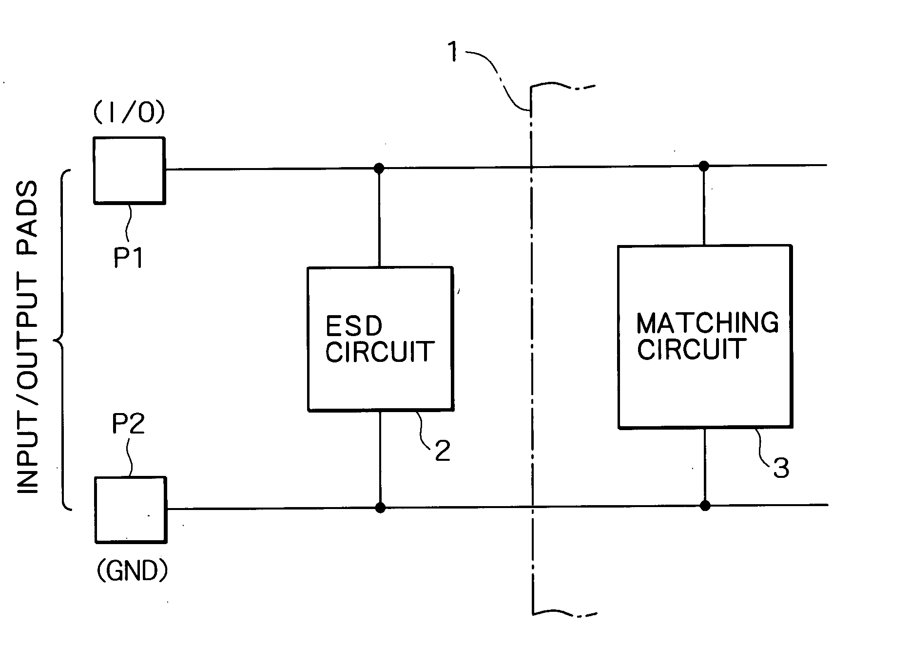
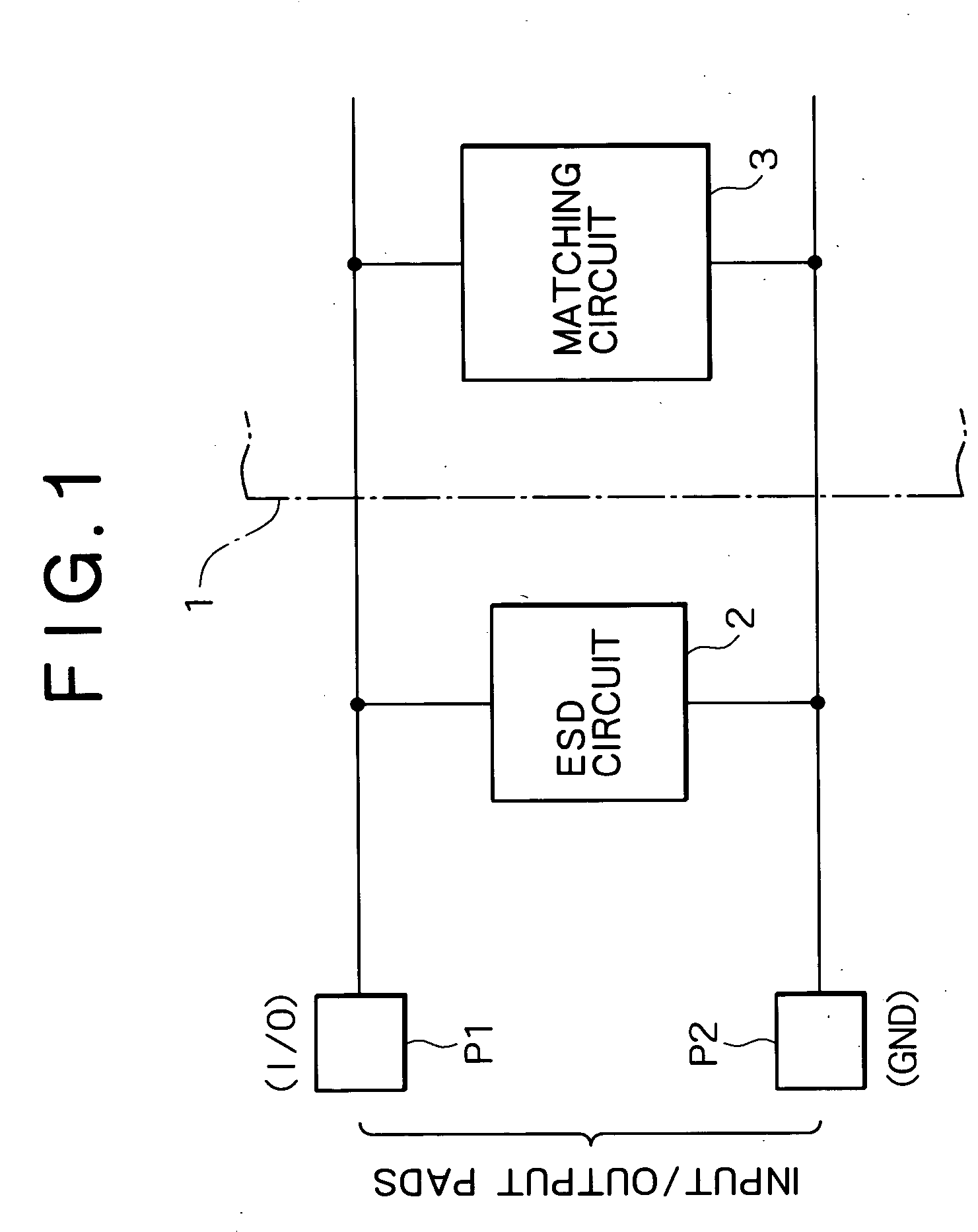
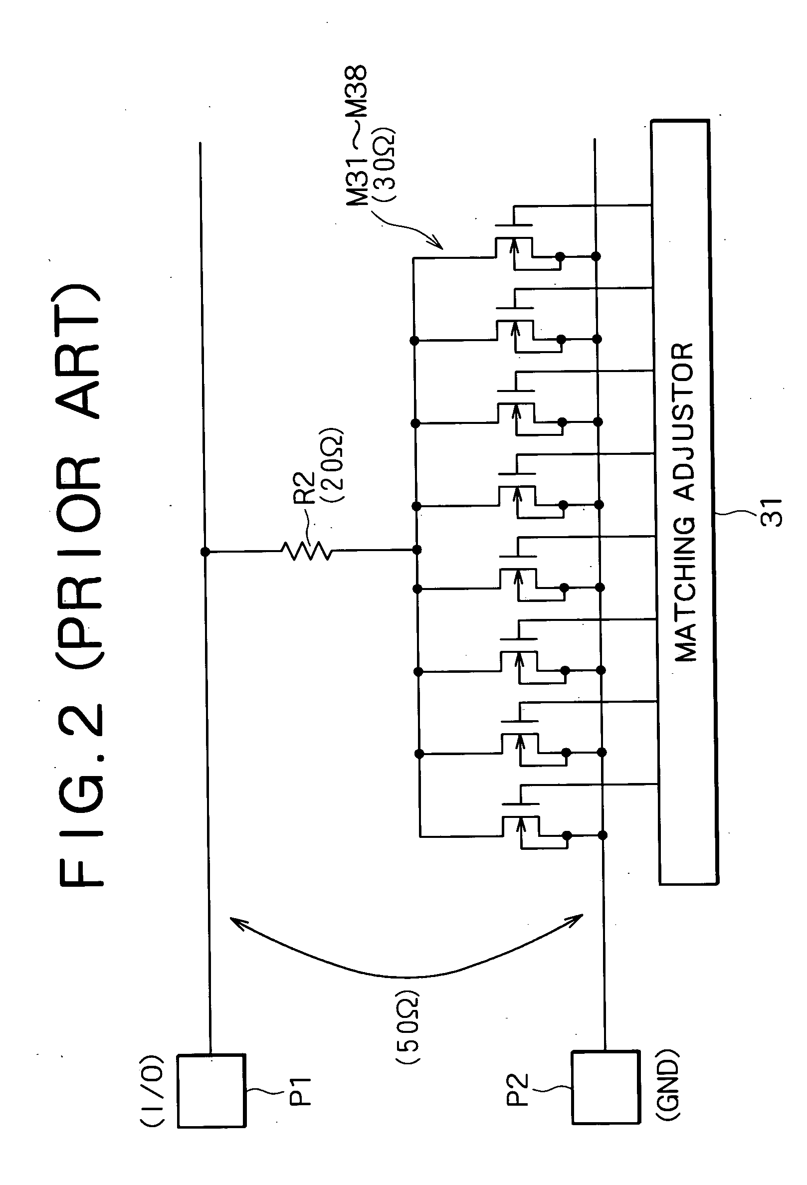
[0032] As shown in FIG. 3A, for example, a ballast resistor R1 and a MOS transistor M1 are connected in series in the ESD circuit 2. Alternatively, as disclosed in Japanese Unexamined Patent Application Publication No. 2001-110995, the ESD circuit 2 may include a plurality of MOS transistors in which the drains thereof are connected to the two pads and the sources are selectively shared. Also, various semiconductor devices, such as a bipolar transistor and a diode, may be used. In the first embodiment, as shown in the cross-sectional view in FIG. 3B, the N-type MOS transistor M1 includes a gate G, and a source S, a drain D, and a channel stopper CS having an N-type impurity diffusion layer formed in a P-type well W. The ballast resistor R1 is connected to the drain D of the MOS transistor M1 and to the I / O pad P1. The source S of the MOS transistor M1 is grounded, that is, connected to the GND pad P2.

[0033] Referring to FIG. 3C, which illustrates the relationship between a surge cur...

second embodiment

[0062] In the second embodiment, each two MOS transistors connected to the resistance elements R11 to R14 are disposed in the respective element regions 11a to 11d. With this configuration, mutual effect of bipolar operation between MOS transistors in different element regions can be avoided. Further, by providing the MOS transistors separately in the four element regions, the degree of freedom in the layout of the MOS transistors M11 to M18 and the resistance elements R11 to R14 can be increased, which results in simplification of design and high integration.

[0063] Next, a semiconductor IC device according to a third embodiment of the present invention will be described. FIG. 7 is a circuit diagram showing a matching circuit according to the third embodiment. In the third embodiment, each three (m=3) MOS transistors M11 to M13, M14 to M16, M17 to M19, and M20 to M22 connected in parallel are connected in series to the four resistance elements R11 to R14, respectively, and each resi...


PUM


Abstract

A semiconductor IC device includes an electrostatic protective circuit connected to an internal circuit connected between two pads. The internal circuit includes a matching circuit for adjusting the impedance between the two pads. The matching circuit includes n (n is a positive number of 2 or more) resistance elements connected in parallel between the two pads; n×m (m is a positive number of 2 or more) transistors, each m transistors connected in parallel being connected in series to the n resistance elements, respectively; and an adjustor for selectively allowing the transistors to perform an ON-operation. The resistance of each resistance element is set to a larger value than the impedance to be adjusted. Accordingly, a surge-current control effect is enhanced and breakdown of the transistors can be prevented.

Description

BACKGROUND OF THE INVENTION [0001] 1. Field of the Invention [0002] The present invention relates to a semiconductor integrated circuit (IC) device, in particular, to a semiconductor IC device configured so that electrostatic breakdown of a transistor placed in the input / output side of an internal circuit is prevented. [0003] 2. Description of the Related Art [0004] In a semiconductor IC device, as shown in FIG. 1, in order to prevent electrostatic discharge (ESD) breakdown in an internal circuit 1 caused by static electricity applied between two pads P1 and P2 including a power-supply pad and a signal input / output pad, an ESD circuit 2 is provided in series or parallel with a circuit for connecting the internal circuit 1 and the two pads P1 and P2. The ESD circuit 2 dissipates an ESD surge current (hereinafter referred to as a surge current) from a high-potential pad (for example, a signal input / output pad (I / O pad)) P1 to a low-potential pad (for example, a ground pad (GND pad)) P...

Claims


Application Information

Patent Timeline
Patent Type & Authority Applications(United States)
IPC IPC(8): H01L27/04H01L21/822H01L21/8234H01L27/02H01L27/088H01L29/78
CPCH01L27/0288
Inventor OKUSHIMA, MOTOTSUGU
Owner RENESAS ELECTRONICS CORP
Why Eureka
Try Eureka