MRAM cell with flat topography and controlled bit line to free layer distance and method of manufacture

a technology of mram cell and flat topography, which is applied in the direction of substrate/intermediate layer, spin-exchange-coupled multilayer, instruments, etc., can solve the problems of preventing satisfactory lifting off of the mask, affecting the production efficiency of the mram device, and affecting the quality of the mram device. , to achieve the effect of enhancing the magnetic field production, preventing the degradation of the characteristics of the mram device, and reducing the mram devi

Active Publication Date: 2005-06-16
TAIWAN SEMICON MFG CO LTD
View PDF4 Cites 19 Cited by
  • Summary
  • Abstract
  • Description
  • Claims
  • Application Information

AI Technical Summary

Benefits of technology

[0015] The disadvantageous effects of non-uniformly formed device surfaces is particularly severe when such devices are to be directly integrated into associated microelectronic circuitry. Durlam et al. (U.S. Pat. No. 6,174,737 B1) disclose an MRAM device with associated CMOS circuitry and they note (column 1, line 62) the necessity of forming flat surfaces to “prevent the characteristics of an MRAM device from degrading.” Durlam et al. teach the use of CMP processes (column 2, line 32) to produce a flat surface. They also teach the enclosure of word and bit lines in permalloy covers to enhance their magnetic field production.
[0016] Pan et al. (U.S. Pat. No. 6,548,849 B1) teach a method for forming an MRAM device surrounded by a magnetic yoke whose purpose is to reduce the current required to change states in the junction. Although this method addresses issues relating to power consumption in MRAM structures, it does not address the basic formation problems of smooth upper device surfaces and controllable distances between current carrying lines and the free layer of the device.
[0017] A first object of this invention is to provide a method for forming MRAM cell structures that avoids the uncontrollable variations in surface topography that result from conventional lift-off processes used in patterning the cell.
[0018] A second object of this invention is to provide a method for forming MRAM cell structures that avoids the uncontrollable variations in surface topography that result from conventional CMP processes used in planarizing the cell and surrounding insulation layers.
[0019] A third object of this invention is to provide a method for forming MRAM cell structures that allows controllability of the distance between the current carrying word line and the free layer of the cell element, the bit line and the free layer of the cell element or both the word and bit lines and the free layer of the cell element.
[0020] A fourth object of the present invention is to provide a method of forming MRAM cells that are too small to be formed by conventional processes.

Problems solved by technology

If the undercut is insufficient, dielectric material will build up against the mask sides, as is shown here, and prevent a satisfactory lifting off of the mask.
If the undercut is too great, the mask will become unstable or lift off before the IBE process.
Therefore, there is a limit on the degree to which the process can be extended to smaller devices.
The fluctuations from planarity in the resultant topography (95) are highly disadvantageous for the formation of future device structures upon that topography.
The variations in the topography become more extreme and uncontrollable as further lift-off processes are used.
The inability to control the thickness of the capping layer during CMP translates into an inability to control the distance between a word line (and / or a bit line) formed on the capping layer and the free layer within the junction (s).
Since the strength of the switching field at the free layer produced by current in the word (or bit) line is dependent on the distance between the word (or bit) line and the free layer, these uncontrollable distances produce a non-uniformity in the behavior of the MRAM devices.
The disadvantageous effects of non-uniformly formed device surfaces is particularly severe when such devices are to be directly integrated into associated microelectronic circuitry.
Although this method addresses issues relating to power consumption in MRAM structures, it does not address the basic formation problems of smooth upper device surfaces and controllable distances between current carrying lines and the free layer of the device.

Method used


Image

  • MRAM cell with flat topography and controlled bit line to free layer distance and method of manufacture
  • MRAM cell with flat topography and controlled bit line to free layer distance and method of manufacture
  • MRAM cell with flat topography and controlled bit line to free layer distance and method of manufacture

Examples


Embodiment Construction

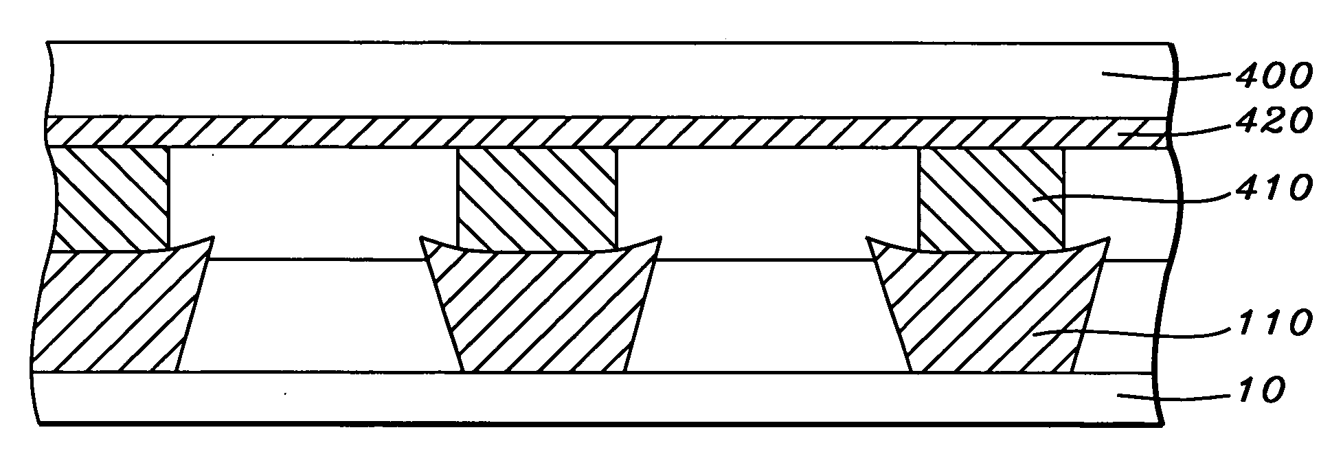
[0028] The preferred embodiment of the present invention is a method of forming an MRAM cell (or an array of such cells) having a magnetic tunnel junction (MTJ) cell element, so that the cell topography is flat and the distance between the word line and the free layer within the element, the distance between the bit line and the free layer within the cell element or the distances between both the word and bit lines and the free layer within the cell element is well controlled. There is also provided the MRAM cell so formed.

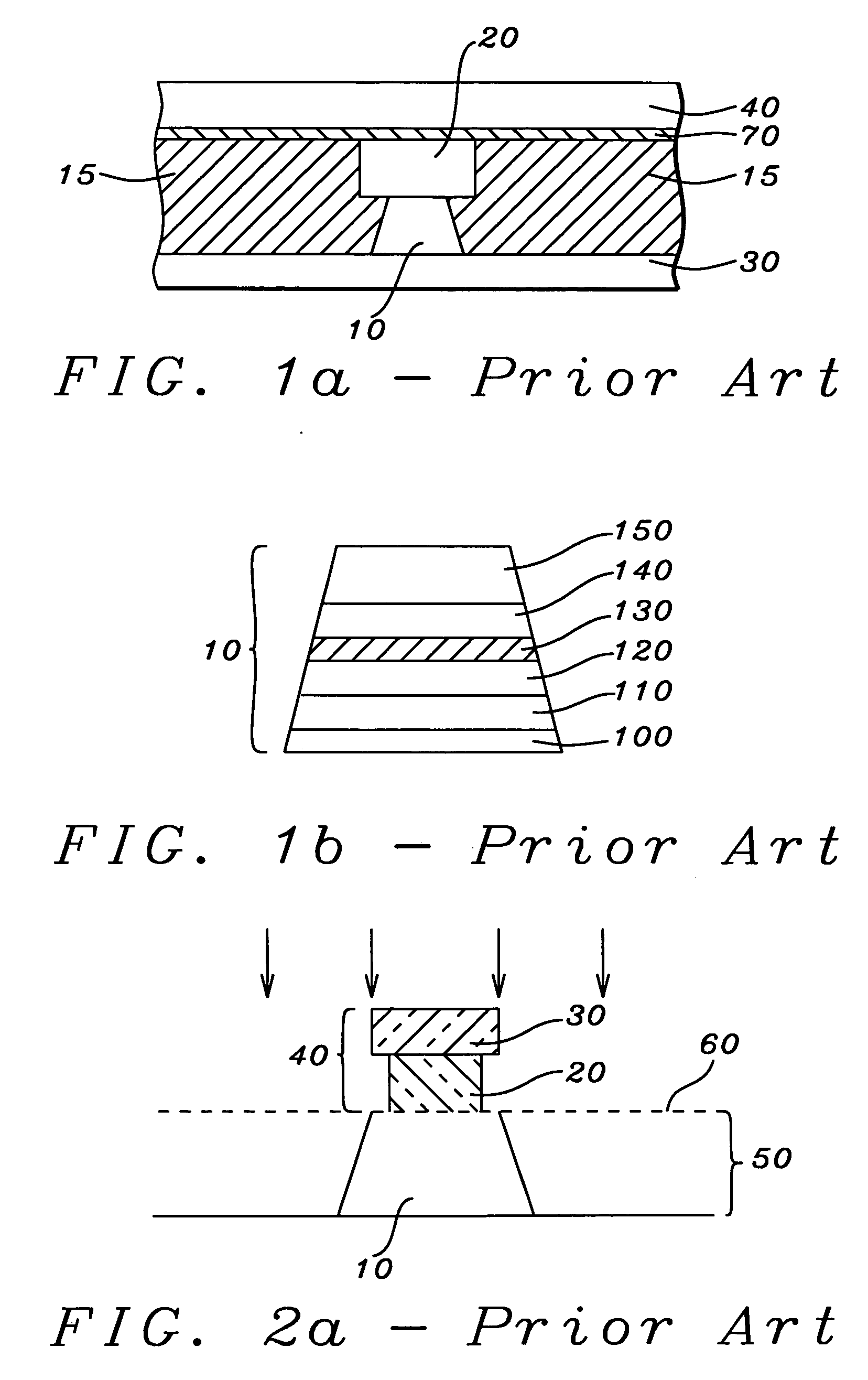
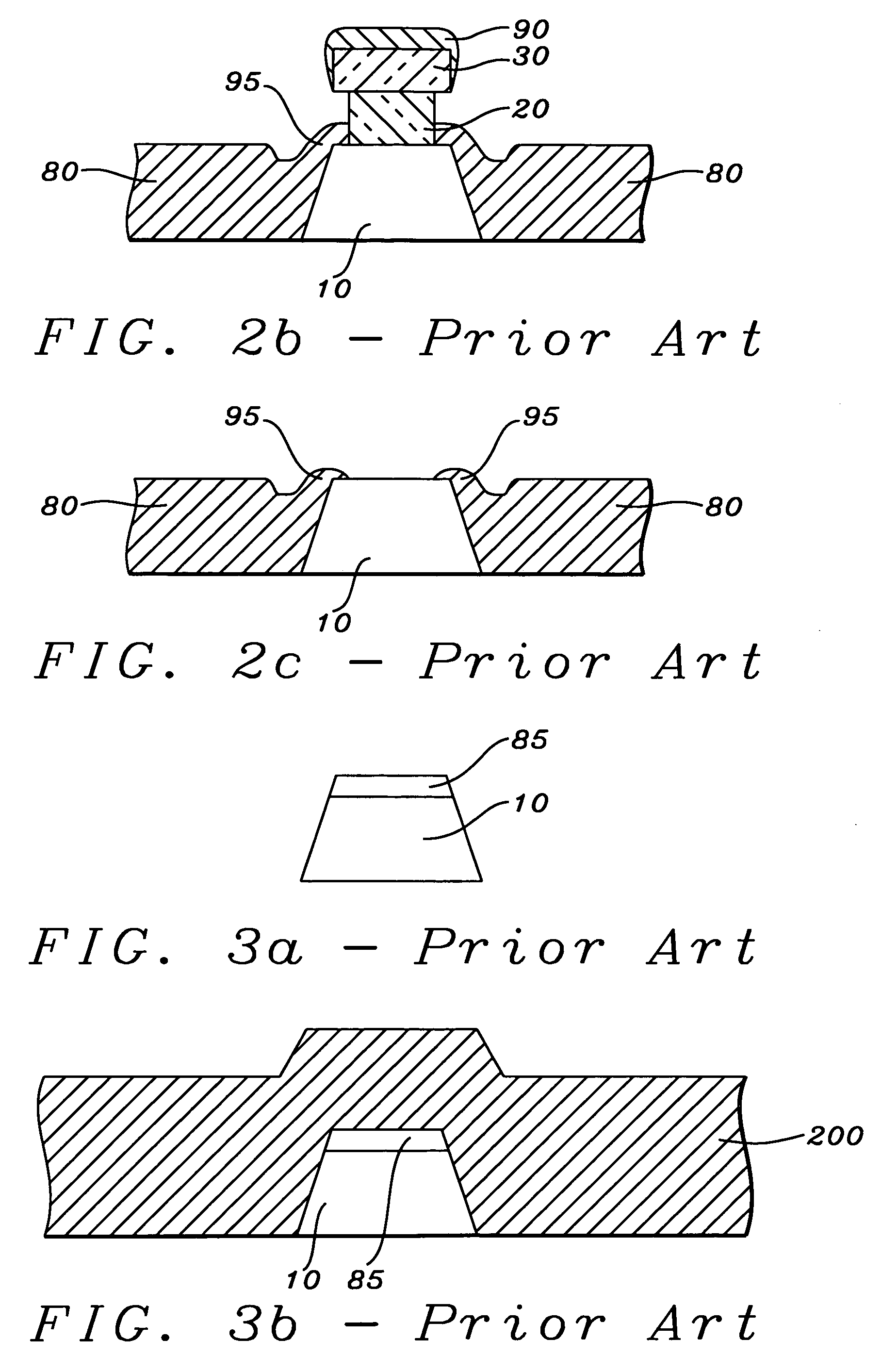
[0029] Referring first to FIG. 4a, there is shown a substrate (10) upon which has been formed an MTJ film stack (20) (the “stack” being the laminated film structure which will subsequently be patterned to form one or a plurality of cell elements) augmented by the addition of capping (80) and sacrificial (90) layers in accord with the present method. The film stack comprises the following lamination of layers, going from bottom to top: a seed layer (30) which may ...


PUM

PropertyMeasurementUnit
thicknessaaaaaaaaaa
thicknessaaaaaaaaaa
thicknessaaaaaaaaaa

Abstract

A method for forming MRAM cell structures wherein the topography of the cell is substantially flat and the distance between a bit line and a magnetic free layer, a word line and a magnetic free layer or a word line and a bit line and a magnetic free layer is precise and well controlled. The method includes the formation of an MTJ film stack over which is formed both a capping and sacrificial layer. The stack is patterned by conventional means, then is covered by a layer of insulation which is thinned by CMP to expose a remaining portion of the sacrificial layer. The remaining portion of the sacrificial layer can be precisely removed by an etching process, leaving only the well dimensioned capping layer to separate the bit line from the magnetic free layer and the capping layer. The bit line and an intervening layer of insulation separate the free layer from a word line in an equally precise and controlled manner.

Description

BACKGROUND OF THE INVENTION [0001] 1. Field of the Invention [0002] This invention relates generally to the fabrication of MRAM device structures and particularly to a structure having a flat topography and a controlled distance between the free layer of the magnetic junction and the bit line, the word line or both. [0003] 2. Description of the Related Art [0004] A magnetic random access memory (MRAM) cell generally consists of a magnetic junction portion that is formed between at least two current carrying lines and surrounded by an insulating layer. The magnetic junction portion of the cell is capable of storing information as a result of it having different resistance states. The different resistance states can be set by a write operation and identified by a read operation by means of multiple current carrying lines (in a simple configuration, a bit line and a word line) that contact the junction at opposite ends. More specifically, if the magnetic junction portion of the cell is...

Claims


Application Information

Patent Timeline
Patent Type & Authority Applications(United States)
IPC IPC(8): G11C11/14H01F10/32H01L21/8246H01L27/105H01L27/22H01L29/82H01L31/062H01L43/08H01L43/12
CPCH01L43/12H01L27/222H10B61/00H10N50/01
Inventor HAN, CHERNG-CHYIHONG, LIUBO
Owner TAIWAN SEMICON MFG CO LTD
Why Eureka
Try Eureka