Wafer acceptance testing method and structure of a test key used in the method

a testing key and acceptance technology, applied in semiconductor/solid-state device testing/measurement, semiconductor/solid-state device details, instruments, etc., can solve the problems of difficult for an inspector to judge the gc-dt misalignment merely according, and the prior art gc-dt misalignment evaluation method is not accura

Active Publication Date: 2005-06-16
NAN YA TECH
View PDF13 Cites 13 Cited by
  • Summary
  • Abstract
  • Description
  • Claims
  • Application Information

AI Technical Summary

Benefits of technology

[0007] It is the primary object of the present invention to provide a novel wafer acceptance testing (WAT) method for accurately monitoring GC-DT misalignment.

Problems solved by technology

However, the prior art GC-DT misalignment evaluation method is not accurate because there are so many factors affecting the threshold voltages shift of the GC-T 201 and GC-B 204.
Therefore, it is difficult for an inspector to judge the GC-DT misalignment merely according to the measured threshold voltage shift data.

Method used


Image

  • Wafer acceptance testing method and structure of a test key used in the method
  • Wafer acceptance testing method and structure of a test key used in the method
  • Wafer acceptance testing method and structure of a test key used in the method

Examples


Embodiment Construction

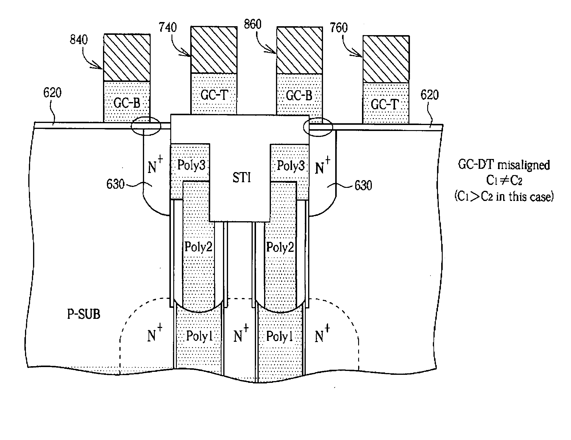
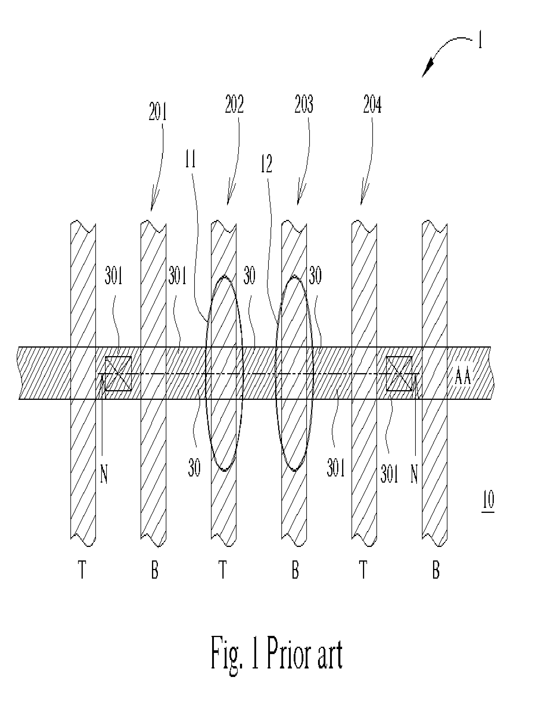
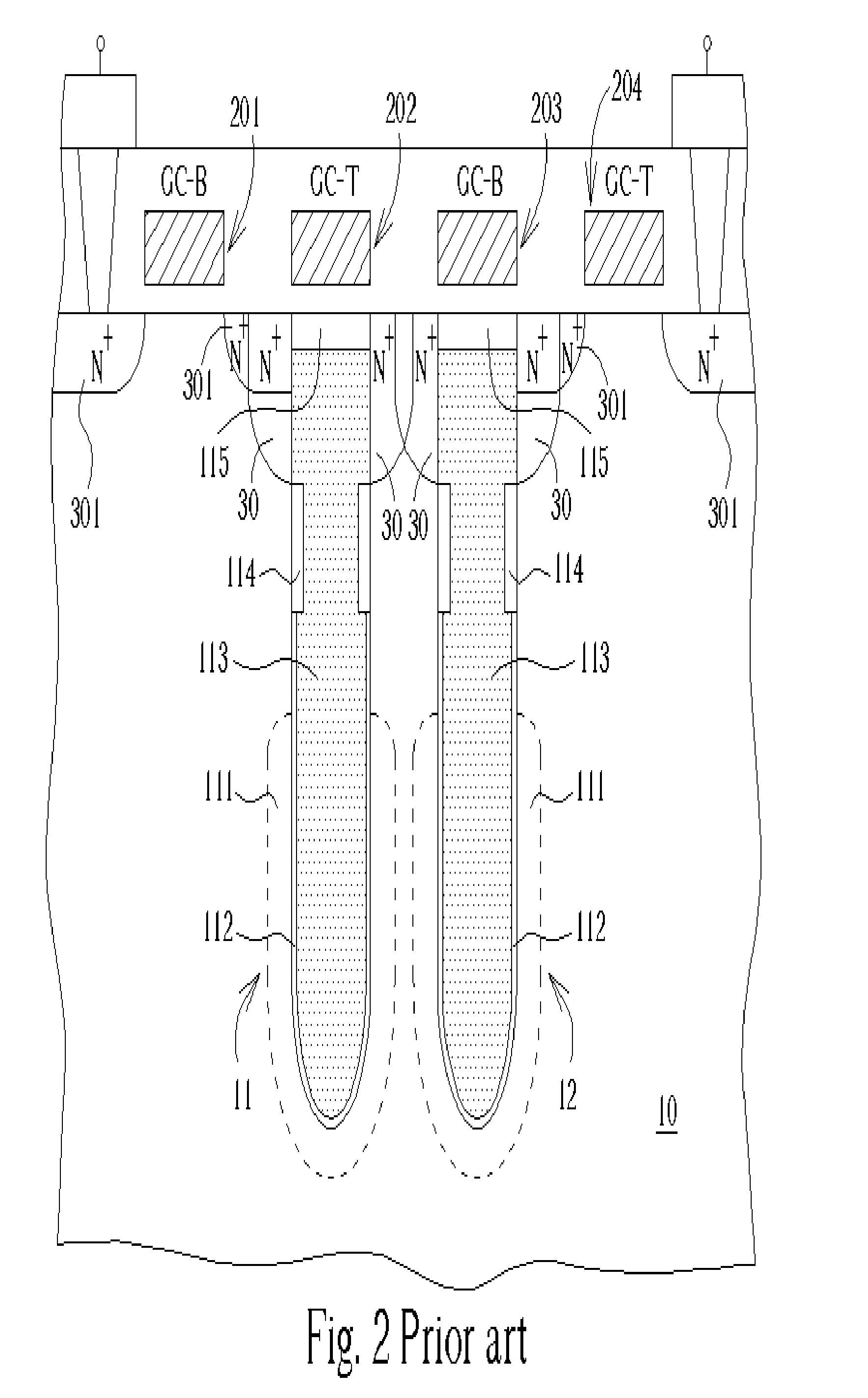
[0015] Please refer to FIG. 3 to FIG. 9. FIG. 3 to FIG. 9 are schematic diagrams illustrating the fabrication processes of making a test key structure for monitoring GC-DT misalignment in accordance with one preferred embodiment of the present invention, wherein FIG. 4 is a cross-sectional view along line A-A of FIG. 3; FIG. 6 is a cross-sectional view along line B-B of FIG. 5; and FIG. 8 is a cross-sectional view along line C-C of FIG. 7. Through FIG. 3 to FIG. 9, similar numerals designate similar devices, regions or elements set forth in FIG. 1 and FIG. 2. The novel wafer acceptance testing (WAT) method using the test key structure of the present invention will also be explained in detail with reference to FIG. 8 and FIG. 9.

[0016] As shown in FIG. 3, a finger-type deep trench layout 20 is fabricated simultaneously with the memory array capacitors (not shown) in a substrate 10 such as a P type silicon substrate. The deep trench layout 20, which is fabricated within a peripheral a...


PUM


Abstract

A wafer acceptance testing (WAT) method for monitoring GC-DT misalignment and a test key structure are disclosed. The test key includes a deep trench capacitor structure biased to a first voltage (VDT). The deep trench capacitor structure is formed in a substrate, on which active areas are defined. The deep trench capacitor structure includes a buried strap out diffusion region that is formed within the active area and is electrically connected to the deep trench capacitor structure. The deep trench capacitor structure is isolated by shallow trench isolation (STI). A GC-T electrode layout and a GC-B electrode layout are formed over the substrate. The GC-T electrode layout, which is biased to a second voltage (VGC-T), includes a plurality of columns of GC-T fingers. The GC-B electrode layout, which is biased to a third voltage (VGC-B), includes a plurality of columns of GC-B fingers that interdigitate the plurality of columns of GC-T fingers over the active areas and STI. A first capacitance C1 of a first capacitor contributed by the plurality of columns of GC-T fingers and the buried strap out diffusion region is measured. A second capacitance C2 of a second capacitor contributed by the plurality of columns of GC-B fingers and the buried strap out diffusion region is measured. The first capacitance C1 and second capacitance C2 are compared, wherein when C1≠C2, GC-DT is misaligned.

Description

BACKGROUND OF INVENTION [0001] 1. Field of the Invention [0002] The present invention relates to a wafer acceptance testing (WAT) method, and more particularly, to a WAT method for monitoring gate conductor-deep trench (GC-DT) misalignment and a test key structure used in this method. [0003] 2. Description of the Prior Art [0004] In semiconductor fabrication, a semiconductor device or an integrated circuit (IC) should be continuously tested in every step so as to maintain device quality. Usually, a testing circuit is simultaneously fabricated with an actual device so that quality of the actual device can be judged by a performance of the testing circuit. The quality of the actual device therefore can be well controlled. Typically, such testing circuit, which is also referred to as “test key”, is disposed on peripheral area of each chip or die. [0005] Please refer to FIG. 1 and FIG. 2. FIG. 1 is an enlarged top view of a part of a conventional test key layout for monitoring GC-DT (Ga...

Claims


Application Information

Patent Timeline
Patent Type & Authority Applications(United States)
IPC IPC(8): G01R31/28H01L21/66H01L23/544H01L23/58H01L29/06H01L31/0328
CPCH01L22/34G01R31/2884
Inventor HSU, PING
Owner NAN YA TECH
Why Eureka
Try Eureka