Method and apparatus for forming an SOI body-contacted transistor

a body-contact transistor and body-contact technology, applied in the field of soi body-contact transistors, can solve the problems of reducing the physical size of the body-contact region or capacitance, reducing the physical size of the body-contact gate, and the use of the dual-gate oxide process does not provide any mechanism to reduce the physical size of the body-contact area, so as to achieve the effect of minimizing parasitic capacitance and gate electrode leakag

Active Publication Date: 2005-06-16
NORTH STAR INNOVATIONS
View PDF1 Cites 68 Cited by
  • Summary
  • Abstract
  • Description
  • Claims
  • Application Information

AI Technical Summary

Benefits of technology

[0009] According to one embodiment of the present disclosure, a method for forming a silicon-on-insulator transistor includes forming an active region overlying an insulating layer, wherein a portion of the active region provides an intrinsic body region. A body tie access region is also formed within the active region, overlying the insulating layer and laterally disposed adjacent the intrinsic body region, making electrical contact to the intrinsic body region. A gate electrode is formed overlying the intrinsic body region for providing electrical control of the intrinsic body region, the gate electrode extending over

Problems solved by technology

Such techniques are unable to reduce the size of the body-tie region or capacitance.
In addition, while the use of a dual-gate oxide process in the body-tie gate reduces a capacitance per unit area somewhat, it however does not reduce the physical size of the body-tie gate.
Furthermore, the use of the d

Method used


Image

  • Method and apparatus for forming an SOI body-contacted transistor
  • Method and apparatus for forming an SOI body-contacted transistor
  • Method and apparatus for forming an SOI body-contacted transistor

Examples


Embodiment Construction

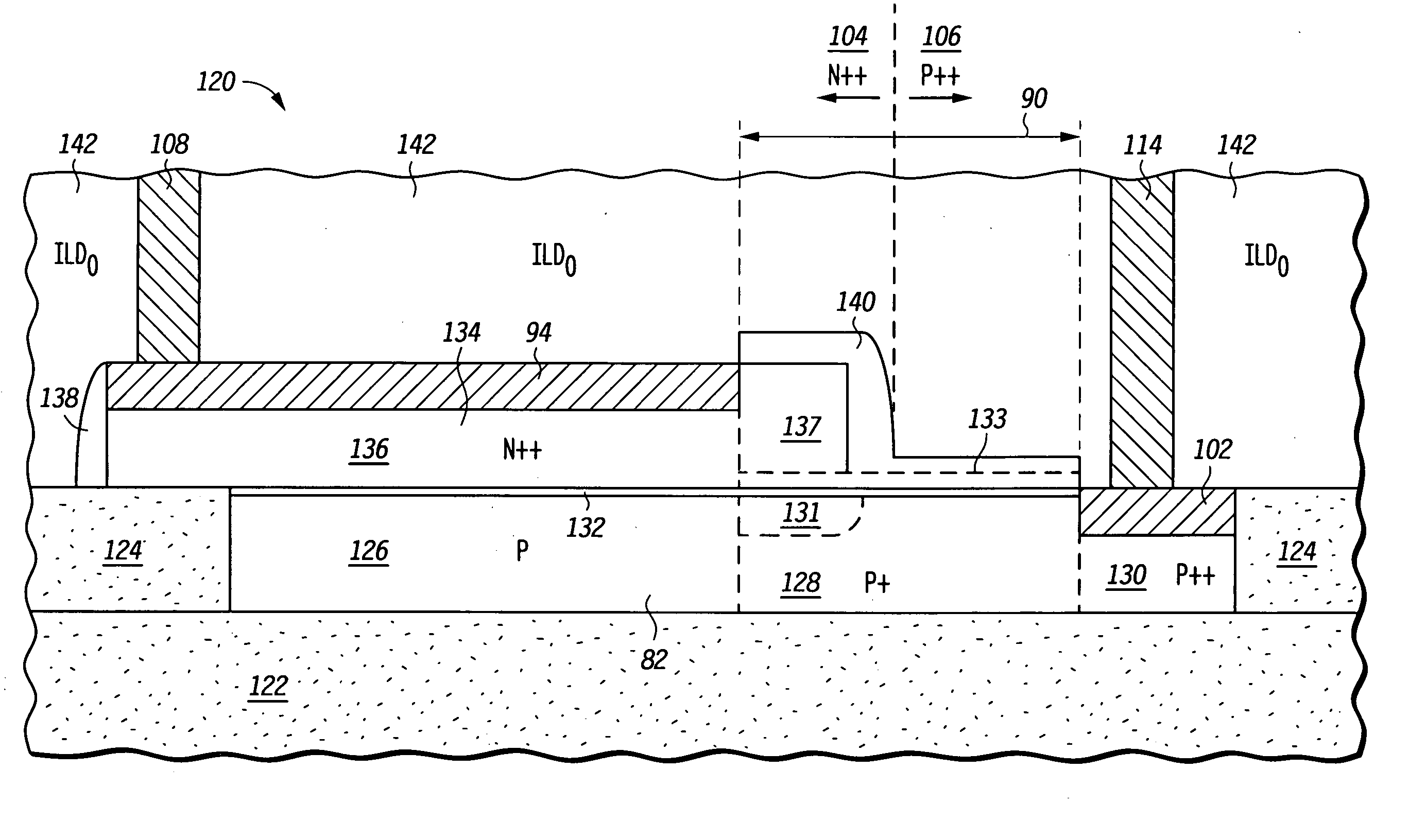
[0022]FIG. 3 is a layout view of a novel SOI body-contacted transistor 80 according to an embodiment of the present disclosure. SOI body-contacted transistor 80 includes an active transistor region 82, wherein active transistor region 82 includes a portion thereof for use as a body tie contact region, as indicated by reference numeral 84. An intrinsic body region, proximate a center of the active transistor region 82, includes a width dimension 86, designated as “W1,” and a length dimension 88, designated as “L1.” A portion of the active region, proximate a center of the body tie region 84, includes a width dimension 90, designated as “W2,” and a length dimension 92, designated as “L2.” This region corresponds to a body tie access region and is designated by reference numeral 128 in FIGS. 3 and 4.

[0023] SOI body-contacted transistor 80 further includes a gate polysilicon 94 overlying the active transistor region 82. The gate polysilicon 94 further includes a portion 96 thereof that...


PUM


Abstract

A method for forming a silicon-on-insulator transistor (80) includes forming an active region (82) overlying an insulating layer (122), wherein a portion of the active region provides an intrinsic body region (126). A body tie access region (128) is also formed within the active region, overlying the insulating layer and laterally disposed adjacent the intrinsic body region, making electrical contact to the intrinsic body region. A gate electrode (134) is formed overlying the intrinsic body region for providing electrical control of the intrinsic body region, the gate electrode extending over a portion (137) of the body tie access region. The gate electrode is formed having a substantially constant gate length (88) along its entire width overlying the intrinsic body region and the body tie access region to minimize parasitic capacitance and gate electrode leakage. First and second current electrodes (98,100) are formed adjacent opposite sides of the intrinsic body region. In addition, a body tie diffusion (130) is formed within the active region and laterally offset from the body tie access region and electrically coupled to the body tie access region.

Description

BACKGROUND [0001] The present disclosure relates generally to semiconductor devices, and more particularly, to a method and apparatus for forming an SOI body-contacted transistor. RELATED ART [0002] Body-contacted SOI transistors are typically built with a polysilicon gate separating the source / drain regions from the body contact region. The additional circuit loading capacitance due to this body-tie gate is substantial, especially for high-performance technologies that use reticle enhancement techniques such as complementary phase-shift masks to reduce the main transistor gate length. Such techniques are unable to reduce the size of the body-tie region or capacitance. [0003] In the prior art, polysilicon gates are used to separate the source / drain regions from the body contact region. Such a layout produces additional gate capacitance sufficient to increase the gate delay, for example, by a factor of 2. In addition, while the use of a dual-gate oxide process in the body-tie gate re...

Claims


Application Information

Patent Timeline
IPC IPC(8): H01L21/20H01L21/336H01L21/84H01L27/01H01L29/45H01L29/786
CPCH01L29/458H01L29/78615H01L29/66772H01L27/12H01L21/18
Inventor VEERARAGHAVAN, SURYADU, YANGWORKMAN, GLENN O.
Owner NORTH STAR INNOVATIONS
Why Eureka
Try Eureka