Method for forming metal wiring of semiconductor device

Inactive Publication Date: 2005-06-16
MAGNACHIP SEMICONDUCTOR LTD
View PDF8 Cites 1 Cited by
  • Summary
  • Abstract
  • Description
  • Claims
  • Application Information

AI Technical Summary

Benefits of technology

[0015] Accordingly, the present invention has been made to solve the above-mentioned problems occurring in the prior art, and an object of the present invention is to provide a method for forming a metal wiring of a semiconductor device capable of reduc

Problems solved by technology

In contrast, when the tungsten CMP process is performed with slurry including a great amount of o

Method used


Image

  • Method for forming metal wiring of semiconductor device
  • Method for forming metal wiring of semiconductor device
  • Method for forming metal wiring of semiconductor device

Examples


Example

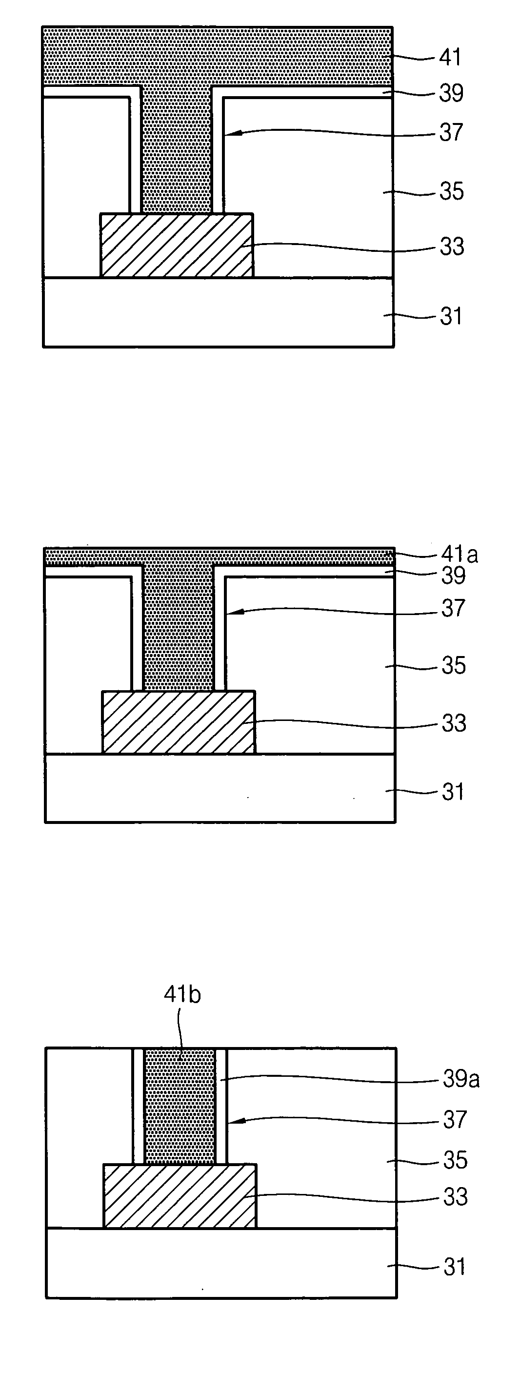
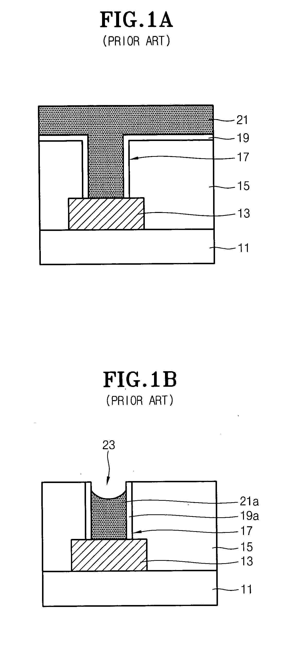
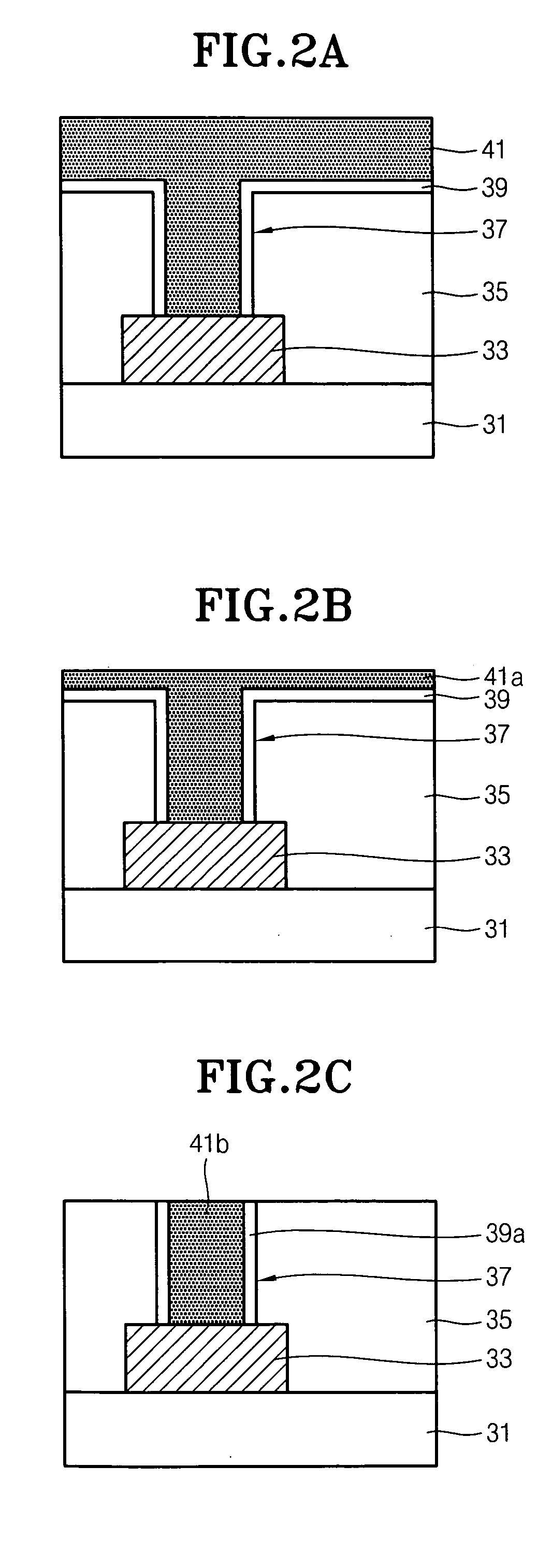
[0025] Hereinafter, a preferred embodiment of the present invention will be described with reference to the accompanying drawings. In the following description and drawings, the same reference numerals are used to designate the same or similar components, and so repetition of the description on the same or similar components will be omitted.

[0026]FIGS. 2A to 2C are sectional views showing process steps for explaining a method of forming a metal wiring of a semiconductor device according to one embodiment of the present invention.

[0027]FIG. 3 is a graph view showing a removal rate for a tungsten layer according to density of H2O2 in a method for forming a metal wiring of a semiconductor device according to one embodiment of the present invention.

[0028] As shown in FIG. 2A, according to the method for forming the metal wiring of the semiconductor device of the present invention, after forming a metal layer pattern 33 on a lower layer 31, and an oxide interlayer 35 is deposited on t...


PUM


Abstract

Disclosed is a method for forming a metal wiring of a semiconductor device. After an oxide interlayer is formed on a lower layer including a metal layer pattern, a contact hole exposing an upper surface of the metal layer pattern is formed in the oxide interlayer. After filling the contact hole by forming a tungsten film on the oxide interlayer including the contact hole, the tungsten film is polished by performing a first CMP process until an upper surface of the oxide interlayer is not exposed. After performing the first CMP process, a second CMP process is performed in such a manner that the tungsten film only remains in the contact hole.

Description

BACKGROUND OF THE INVENTION [0001] 1. Field of the invention [0002] The present invention relates to a method for forming a metal wiring of a semiconductor device, and more particularly to a method for forming a metal wiring of a semiconductor device through carrying out two-step tungsten CMP processes according to density an oxidizing agent included in tungsten slurry. [0003] 2. Description of the Prior Art [0004] Generally, oxidizing agents mainly used in tungsten CMP slurry include H2O2, KlO3, Fe(NO3)3, or H5lO6. [0005] Hereinafter, a conventional method for forming a metal wiring by utilizing such oxidizing agents will be explained with reference to FIGS. 1A and 1B. [0006]FIGS. 1A and 1B are sectional views showing process steps for explaining the conventional method for forming a metal wiring of a semiconductor device. [0007] As shown in FIG. 1A, according to the conventional method for forming the metal wiring, after a metal layer pattern 13 is formed on a lower layer 11, an o...

Claims


Application Information

Patent Timeline
IPC IPC(8): H01L21/28H01L21/44H01L21/4763H01L21/768
CPCH01L21/76877H01L21/7684
Inventor YOON, IL YOUNG
Owner MAGNACHIP SEMICONDUCTOR LTD
Why Eureka
Try Eureka