Memory device signaling system and method with independent timing calibration for parallel signal paths

a memory device and signaling system technology, applied in the field of digital circuits, can solve problems such as complex digital circuits, signal propagation delays, and signals that may be transmitted with a relatively short delay

Inactive Publication Date: 2005-06-16
RAMPART ASSET MANAGEMENT LLC
View PDF93 Cites 96 Cited by
  • Summary
  • Abstract
  • Description
  • Claims
  • Application Information

AI Technical Summary

Benefits of technology

[0013] This invention generally relates to apparatus and methods for timing calibration and device signaling systems in which phase offsets of system device components are not necessarily fixed during normal system operation, but are allowed to vary over a drift range. Systems designed in accordance with the present invention allow for the calibration and adjustment in memory device signaling systems so that the transmission of signal information between a first device (such as for example a memory controller) and a second device (such as for example a memory component) occurs without errors even when the accumulated delays between the first device and second device change by a half symbol time interval or more during operation of the system. This invention can also be utilized for communications between circuit blocks within a single integrated circuit or component.

Problems solved by technology

Today's complex digital circuits contain storage devices, finite-state machines, and other such structures that control the movement of information by various clocking methods.
As signals pass over a bus and through device interfaces, the signals experience propagation delays.
For example, at a low operating temperature with a high supply voltage, signals may be transmitted with a relatively short delay.
Alternatively, at a low supply voltage and high operating temperature, a significantly longer delay may be experienced by transmitted signals.
Variations in the process parameters, which result in variations in the performance of otherwise identical devices, cause devices either on a single bus, or devices on parallel buses to experience different signal propagation delays.
Normally, a variation in propagation delay of even a half symbol time interval will cause a memory system or data transfer system to fail, because movement of a half symbol time will cause the data sample point to move from the center of the data eye to the edge of the data eye.
Change in the propagation delay of more than a half symbol time will, in conventional prior art systems, cause the wrong symbol to be sampled by the receiving device.

Method used


Image

  • Memory device signaling system and method with independent timing calibration for parallel signal paths
  • Memory device signaling system and method with independent timing calibration for parallel signal paths
  • Memory device signaling system and method with independent timing calibration for parallel signal paths

Examples


Embodiment Construction

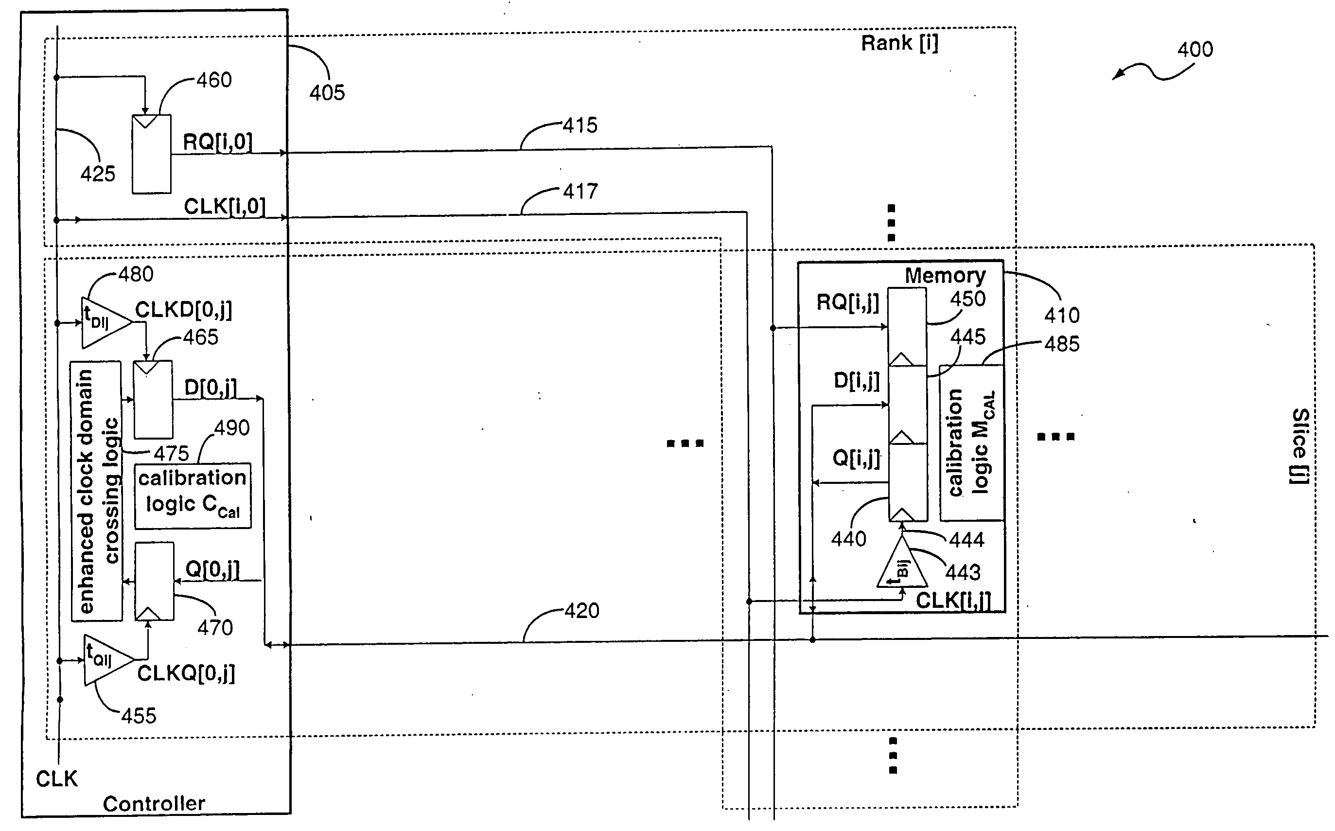
[0060] The term “mesochronous” refers to a relationship between two signals having the same average rate or frequency, but which may have arbitrarily different phases. The term “mesochronous system” refers to a set of clocked components in which the clock signal for each clocked component has the same frequency, but can have a relative phase offset. The term “static mesochronous system” means that the relative phase offsets are fixed and do not vary during normal system operation. The approach of using fixed relative phase offsets that do not vary during normal system operation has been the method practiced in prior art systems. The present invention is directed to “dynamic mesochronous systems” in which the phase offsets of the clocked components are allowed to drift over some range during system operation. The term “normal system operation” is used in this document to refer to ordinary memory access operations, such as read, write and refresh operations. Calibration operations, wh...


PUM


Abstract

A memory system includes a memory controller and a memory component coupled to each other. The memory controller includes an interface to receive a first signal and a second signal from the memory component, wherein the first signal comprises a first symbol and the second signal comprises a second symbol. A first circuit of the memory controller receives the first signal by sampling the first symbol using a first timing offset relative to a reference clock signal, and a second circuit of the memory controller receives the second signal by sampling the second symbol using a second timing offset relative to the reference clock signal. The first timing offset is independent of the second timing offset.

Description

[0001] This application is a division of U.S. patent application Ser. No. 10 / 278,478 filed Oct. 22, 2002, which claimed priority to U.S. provisional application 60 / 343,905, filed on Oct. 22, 2001, and U.S. provisional application 60 / 376,947, filed on Apr. 30, 2002. Application Ser. No. 10 / 278,478, and provisional application 60 / 343,905, and 60 / 376,947, are hereby incorporated by reference.FIELD OF THE INVENTION [0002] This invention generally relates to the field of digital circuits, and more particularly to an apparatus and method for timing calibration and memory device signaling systems. BACKGROUND OF THE INVENTION [0003] Integrated circuits connect to and communicate with each other, typically using a bus with address, data and control signals. Today's complex digital circuits contain storage devices, finite-state machines, and other such structures that control the movement of information by various clocking methods. Transferred signals must be properly synchronized or linked s...

Claims


Application Information

Patent Timeline
Patent Type & Authority Applications(United States)
IPC IPC(8): G11C7/10G11C7/22G11C11/4078H04L7/00
CPCG11C7/10G06F12/0246G11C7/106G11C7/1066G11C7/1078G11C7/1087G11C7/22G11C7/222G11C11/4078G11C2207/2254H04L7/0025H04L7/0079H04L7/0091G11C11/40611G11C21/00G11C7/1051H04L67/10H10B43/27G06F3/061G06F3/0629G06F3/0671G11C11/4072G11C11/4076G11C11/4093
Inventor HAMPEL, CRAIG E.PEREGO, RICHARD E.SIDIROPOULOS, STEFANOS S.TSERN, ELY K.WARE, FREDRICK A.
Owner RAMPART ASSET MANAGEMENT LLC
Why Eureka
Try Eureka