Electrode device for organic device and electronic device having the same

an electronic device and organic technology, applied in the direction of electric discharge lamps, discharge tubes/lamp details, discharge tubes luminescnet screens, etc., can solve the problems of deterioration of elements, limited metal type, and the inability to apply the technique disclosed in the above patent document 1 to the internal electrode of an mpe element, etc., to achieve the effect of improving adhesion with an organic layer of the organic devi

Inactive Publication Date: 2005-06-23
SEMICON ENERGY LAB CO LTD
View PDF97 Cites 30 Cited by
  • Summary
  • Abstract
  • Description
  • Claims
  • Application Information

AI Technical Summary

Benefits of technology

[0013] The electrode for an organic device according to the first invention formed as above uses the electrode material in which a metal having a work function of 4.2 [eV] or less and a metal having a work function of more than 4.2 [eV] are mixed with the one kind of organic compound is used for at least a portion in contact with the organic layer of an organic device, and an electron injection function derived from the metal having a work function of 4.2 [eV] or less or a hole injection function derived from the metal having a work function of more than 4.2 [eV] is performed in accordance with the polarity of voltage applied to the organic layer. Therefore, the electrode can be used as an electrode of either an anode or a cathode of an organic device and moreover used for an organic device which respectively requires an electron injection function for one organic layer and a hole injection function for the other organic layer as an internal electrode of an MPE element. Further, since one kind of organic compound is used for the electrode material, the adhesion with an organic layer of the organic device is also improved.
[0014] The electrode for an organic device according to the second invention is specialized as an internal electrode provided between the first organic layer and the second organic layer. Accordingly, electrons can be injected into the first organic layer with the firs...

Problems solved by technology

As to the alloy electrode of Mg or Li, element deterioration due to oxidation of the electrode or the like is caused, and moreover, there are various limitations.
In a technique disclosed in the above Patent document 1, the electron injection barrier for the light emitting layer from the cathode side can be lowered by providing...

Method used


Image

  • Electrode device for organic device and electronic device having the same
  • Electrode device for organic device and electronic device having the same
  • Electrode device for organic device and electronic device having the same

Examples


embodiment mode 1

[0018] Shown in FIG. 1 is an electrode for an organic device according to Embodiment Mode 1. For example, an electrode structure in FIG. 1(a) is that a metal electrode 101 is formed over an organic layer 100 of the organic device with a carrier injection electrode layer 110 interposed therebetween. As to the carrier injection electrode layer 110, an electrode material in which a metal for electron injection 112 (a metal having a work function of 4.2 [eV] or less) and a metal for hole injection 113 (a metal having a work function of more than 4.2 [eV]) are mixed with one kind of organic compound 111 is layered.

[0019] The thus formed electrode for an organic device uses the carrier injection electrode layer 110 to be joined to the organic layer 100. Accordingly, an electron injection function derived from the metal for electron injection 112 or a hole injection function derived from the metal for hole injection 113 is performed in accordance with the polarity of the voltage applied t...

embodiment mode 2

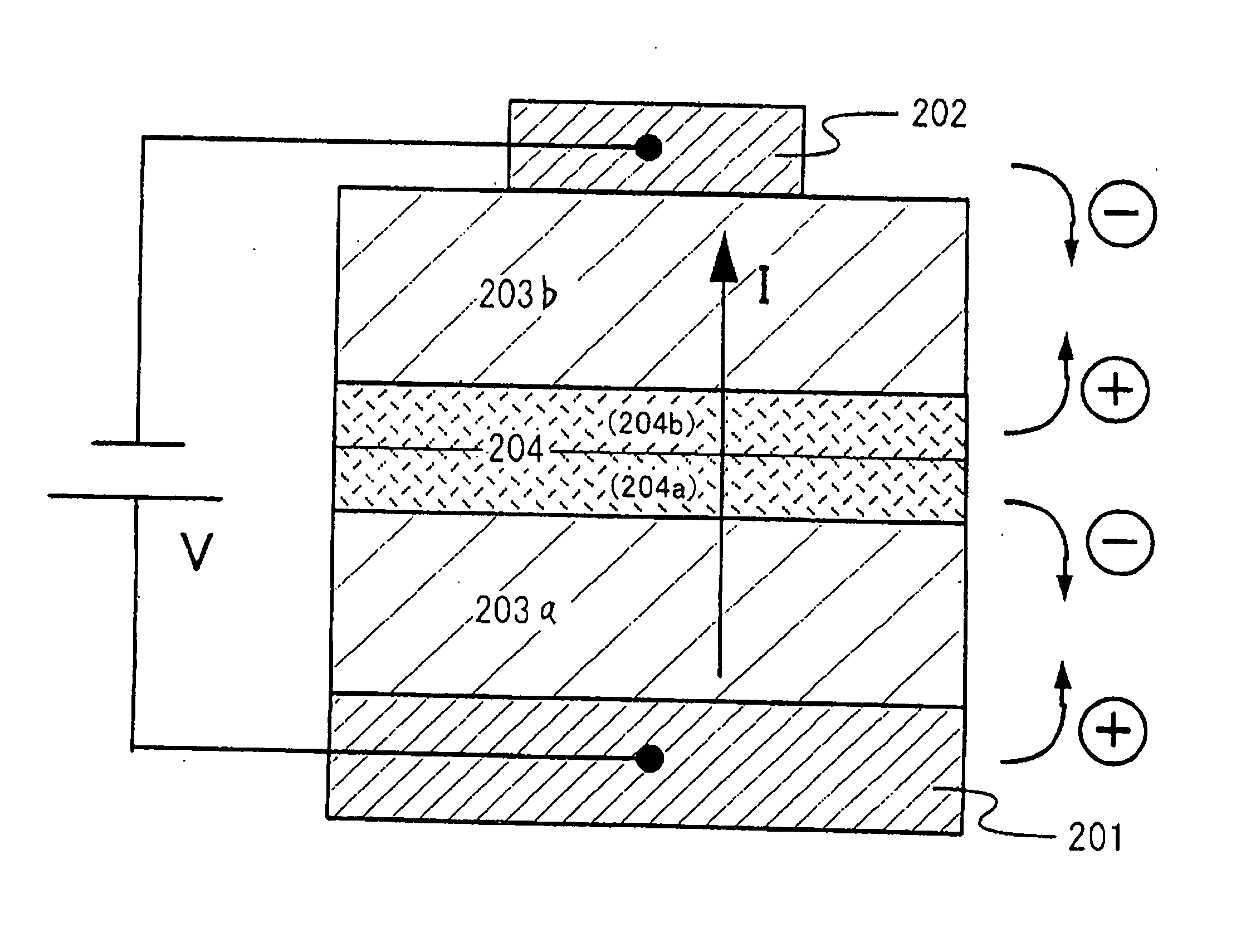
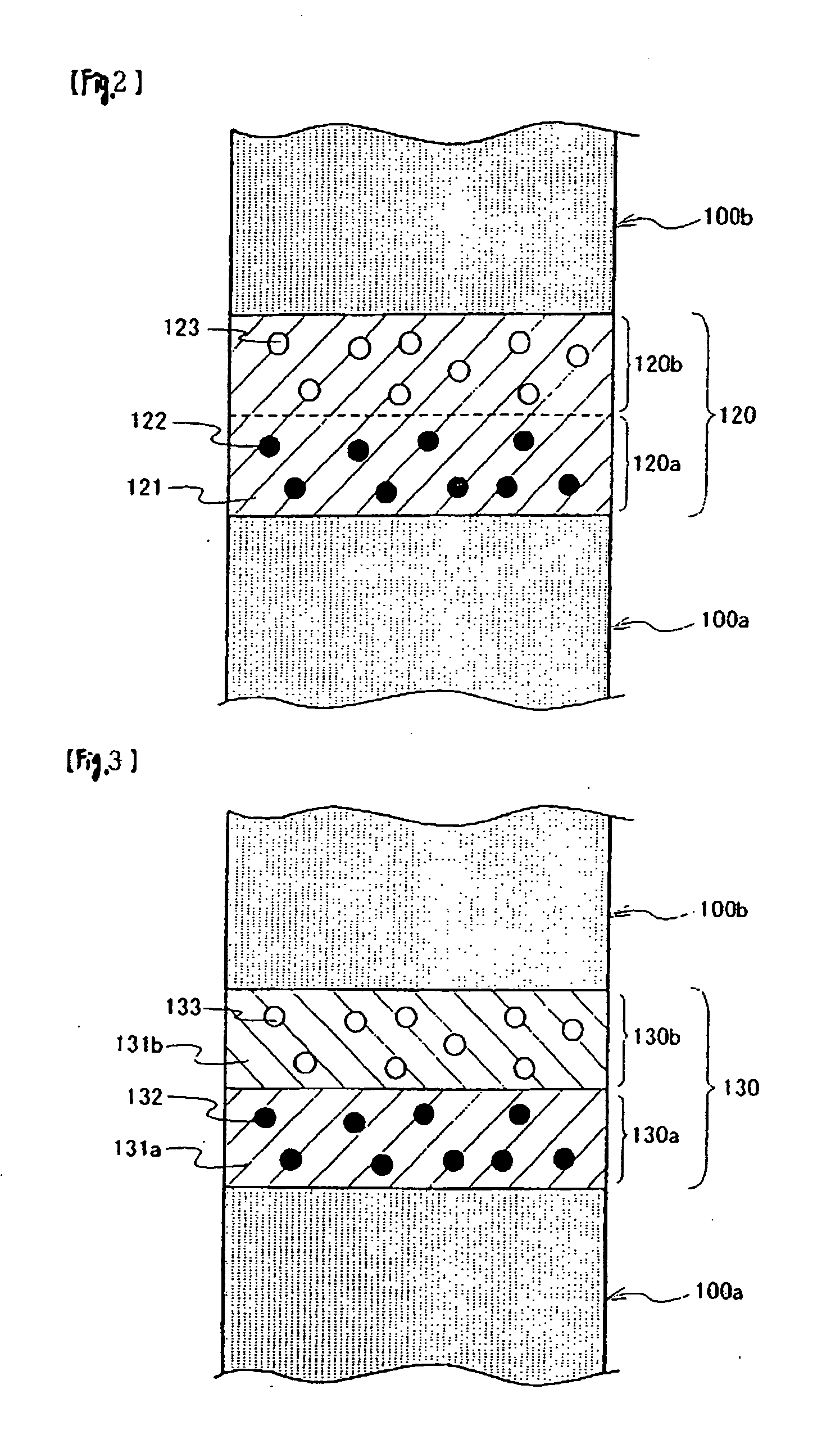
[0024] Next, Embodiment Mode 2 of an electrode for an organic device according to the invention will be described referring to FIG. 2. The structure of the electrode for an organic device according to Embodiment Mode 2 is that an electrode layer 120 is provided between a first organic layer 100a and a second organic layer 10b. The electrode layer 120 is formed as follows: an electron injection region 120a containing a metal for electron injection 122 (having a work function of 4.2 [eV] or less) is formed on the side of one kind of organic compound 121 in contact with the first organic layer 100a, and a hole injection region 120b containing a metal for hole injection 123 (having a work function of more than 4.2 [eV]) is formed on the side of the one kind of organic compound 121 in contact with the second organic layer 100b.

[0025] As to the thus formed electrode for an organic device, when voltage is applied from the side of the first organic layer 100a to the side of the second orga...

embodiment mode 3

[0028] Next, Embodiment Mode 3 of an electrode for an organic device according to the invention will be described referring to FIG. 3. The structure of electrode for an organic device according to Embodiment Mode 3 is that a laminated electrode 130 is provided between a first organic layer 100a and a second organic layer 100b. The laminated electrode 130 is formed as follows: an electron injection electrode layer 130a in which a metal for electron injection 132 (a metal having a work function of 4.2 [eV] or less) is mixed with an organic compound for electron transport 131a is laminated on the side of the first organic layer 100a, and a hole injection electrode layer 130b in which a metal for hole injection 133 (a metal having a work function of more than 4.2 [eV]) is mixed with an organic compound for hole transport 131b is laminated on the side of the second organic layer 100b.

[0029] As to the thus formed electrode for an organic device, when voltage is applied from the side of t...


PUM


Abstract

[Object] To provide an electrode for an organic device which can be widely applied to organic devices by having both hole injection function and electron injection function.
[Solution] A carrier injection electrode layer 110 in which a metal for electron injection 112 (a metal having a work function of 4.2 [eV] or less) and a metal for hole injection 113 (a metal having a work function of more than 4.2 [eV]) are mixed with one kind of organic compound 111 is provided between a first organic layer 100a and a second organic layer 100b. Thus, carriers are injected into a carrier injection electrode layer 110 in the direction according to voltage application, and seemingly, current flows between an organic layer 100 and a metal electrode 101, or between the first organic layer 100a and the second organic layer 100b.

Description

TECHNICAL FIELD [0001] The present invention relates to an electrode for an organic device used for an organic device such as an EL element, FET, which use the properties of an organic compound; and to an electronic device having the electrode for the organic device. BACKGROUND ART [0002] As an organic device, an EL element is widely known. The EL element has an organic compound as a light emitting layer, and current is applied to the light emitting layer by applying voltage by a pair of electrodes provided so as to sandwich the light emitting layer, and photons in accordance with the current density are released; thus, the EL element serves as a light source. In applying voltage to the light emitting layer in an EL element, an alloy of Mg (magnesium) and Ag (silver) or an alloy of Li (lithium) and Al (aluminum), each of the elements has low work function, has been used for a metal electrode of a cathode side in order to lower the electron injection barrier against an organic compou...

Claims


Application Information

Patent Timeline
IPC IPC(8): H01J1/62H01J63/04H01L51/52H05B33/14H05B33/26
CPCH01L51/0021H01L51/5278H01L51/5203H01L51/0512H10K71/60H10K10/462H10K50/19H10K59/805H10K50/805
Inventor TSUTSUI, TETSUOKUMAKI, DAISUKE
Owner SEMICON ENERGY LAB CO LTD
Why Eureka
Try Eureka