

Display device and manufacturing method thereof
- Summary
- Abstract
- Description
- Claims
- Application Information
AI Technical Summary
Benefits of technology
Problems solved by technology
Method used
Image

Examples
embodiment mode 1
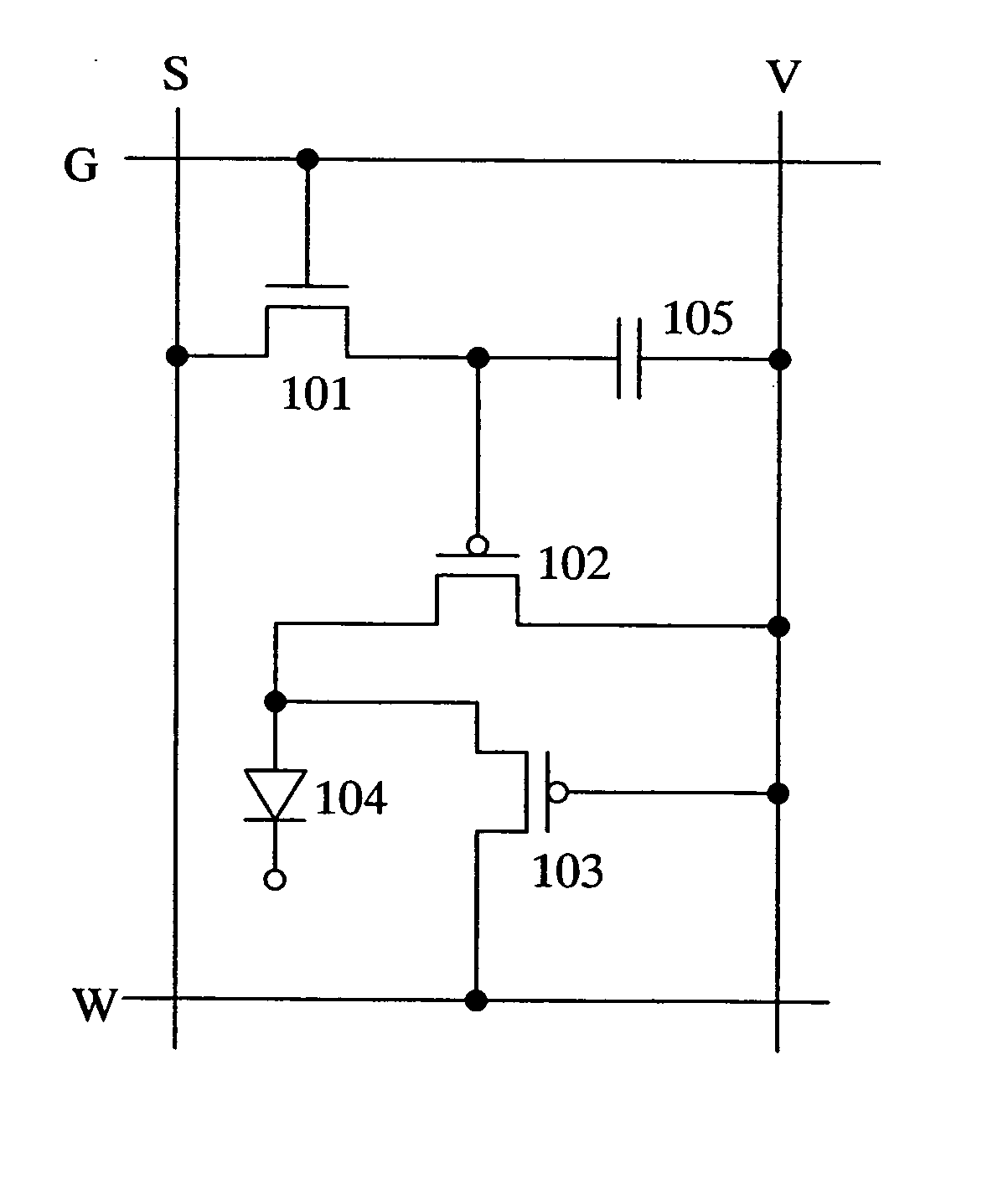
[0049] One embodiment mode of the invention is shown in FIG. 1.
[0050]FIG. 1 shows one embodiment mode of a pixel in a light emitting device of the invention. The pixel shown in FIG. 1 includes a light emitting element 104, a transistor (a switching transistor) 101 serving as a switching element for controlling input of a video signal into the pixel, a driving transistor 102 for controlling the amount of current supplied to the light emitting element 104, and an AC transistor 103 for supplying current to be supplied to the light emitting element 104 when reverse driving voltage for a light emitting element being applied to the light emitting element 104. In addition, as is in this embodiment mode, a capacitor 105 for storing potential of a video signal may be provided in the pixel.
[0051] In this specification, a light emitting element means an element (OLED element) having a structure in which an electroluminescent layer that emits light as an electric field occurs is interposed be...
embodiment mode 2
[0080] An embodiment mode of a pixel in a light emitting device of the invention is described below, which is different from FIG. 1.
[0081] A pixel shown in FIG. 5 includes a light emitting element 504, a switching transistor 501, a driving transistor 502, and an AC transistor 503. A capacitor 505 may be provided in the pixel in addition to the above elements.
[0082] The polarity of the driving transistor 502 and the AC transistor 503 are identical to each other.
[0083] In this embodiment mode, L / W of the driving transistor 502 is set larger than that of the AC transistor 503 to operate the driving transistor 502 in the saturation region and the AC transistor 503 in the linear region. More specifically, the driving transistor 502 is formed such that L is larger than W and IIW thereof is preferably 5 / 1 or more. The AC transistor 503 is formed such that L is equal to or smaller than W.
[0084] In FIG. 5, the switching transistor 501 is an n-channel transistor whereas the driving transi...
embodiment 1
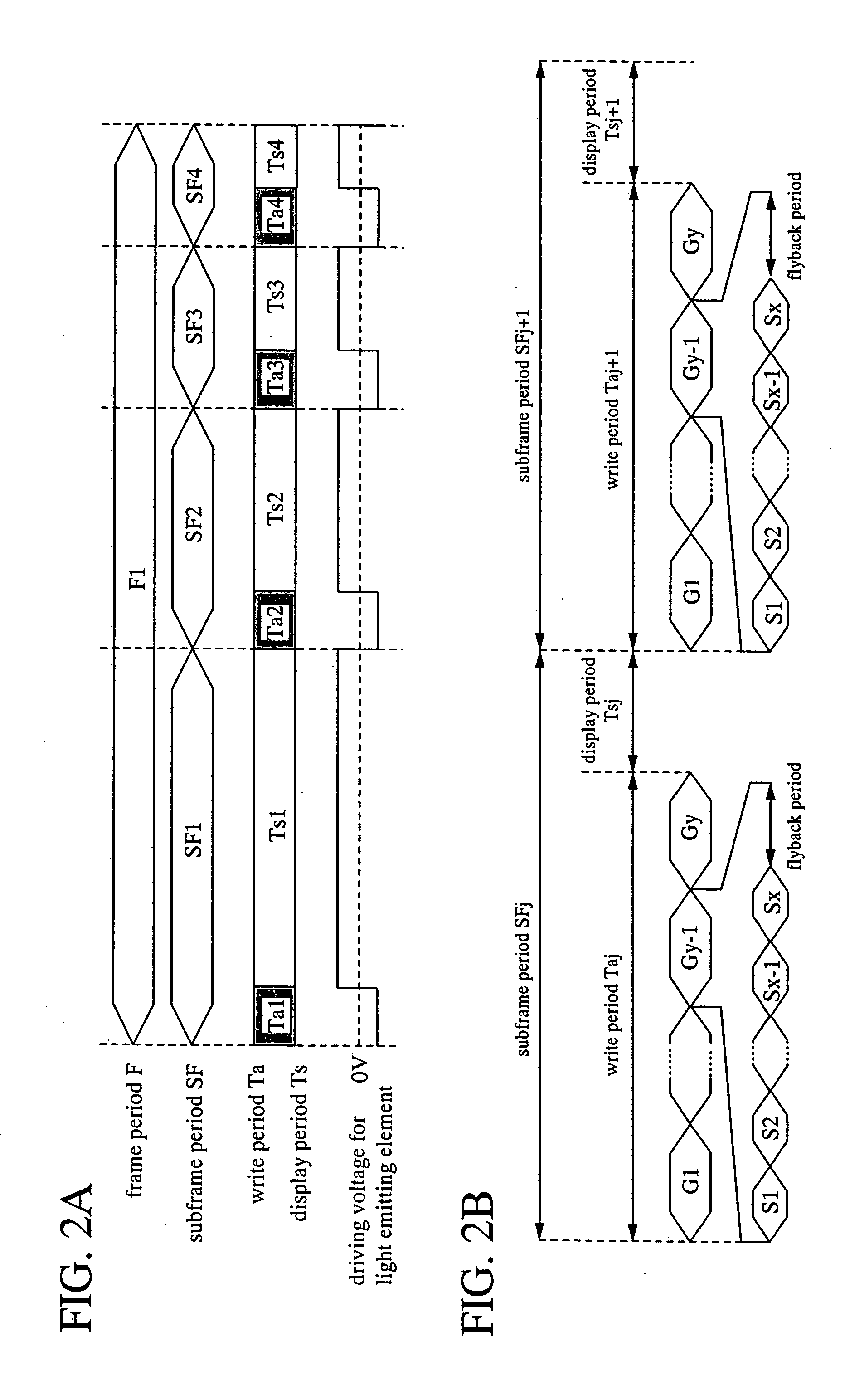
[0093] Described with reference to FIG. 6 is a circuit for inputting signals to a source signal line driving circuit and a gate signal line driving circuit of a display to operate the display with a digital time gray scale method.
[0094] In this embodiment, a display device inputted with a 4-bit digital video signal to display an image is described. Note that the invention is not limited to a case of 4-bit.
[0095] A signal control circuit 601 is inputted with digital video signals and outputs digital video signals VD to a display 600.
[0096] In this embodiment, digital video signals are compiled in the signal control circuit 601. A digital video signal after being converted to be inputted to a display is called a digital video signal VD.
[0097] Signals and driving voltage for operating a source signal line driving circuit 607 and a gate signal line driving circuit 608 of the display 600 are inputted by a display controller 602.
[0098] Respective configurations of the signal control ...
PUM
 Abstract
Description
Claims
Application Information