Method to monitor silicide formation on product wafers

a technology of product wafers and silicides, applied in electrical testing, electronic circuit testing, instruments, etc., can solve the problems of low production efficiency, low efficiency, and high cost of the present method of metal silicide monitoring

Inactive Publication Date: 2005-06-23
CHARTERED SEMICONDUCTOR MANUFACTURING
View PDF9 Cites 26 Cited by
  • Summary
  • Abstract
  • Description
  • Claims
  • Application Information

AI Technical Summary

Benefits of technology

[0009] A principal object of the present invention is to provide an effective and very manufacturable method to monitor a metal silicide process in an integrated circuit device.

Problems solved by technology

Second, the sheet resistance measurements of the monitors are obscured by batch-to-batch variations, particularly after the deposition of titanium and / or titanium nitride and the first rapid thermal anneal (RTA) process.
Therefore, the present method of metal silicide monitoring is expensive and generates less than optimal results.

Method used


Image

  • Method to monitor silicide formation on product wafers
  • Method to monitor silicide formation on product wafers
  • Method to monitor silicide formation on product wafers

Examples


Embodiment Construction

[0023] The preferred embodiments of the present invention disclose a method to monitor the metal silicide process in the manufacture of an integrated circuit device. An optical measurement system is used to derive an electronic signal from product wafers. This electronic signal linearly corresponds to sheet resistance and is used in the present invention as a means of monitoring the metal silicide process. It should be clear to those experienced in the art that the present invention can be applied and extended without deviating from the scope of the present invention.

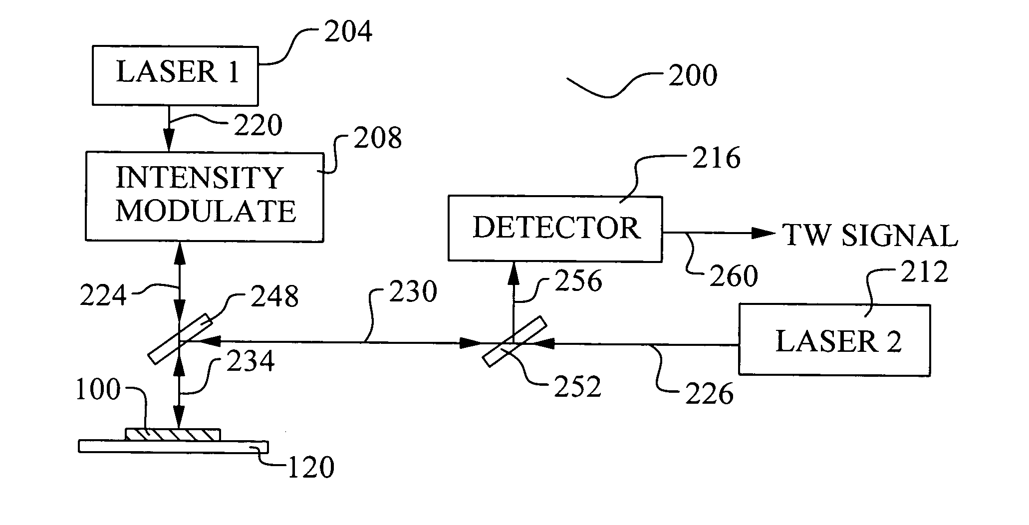
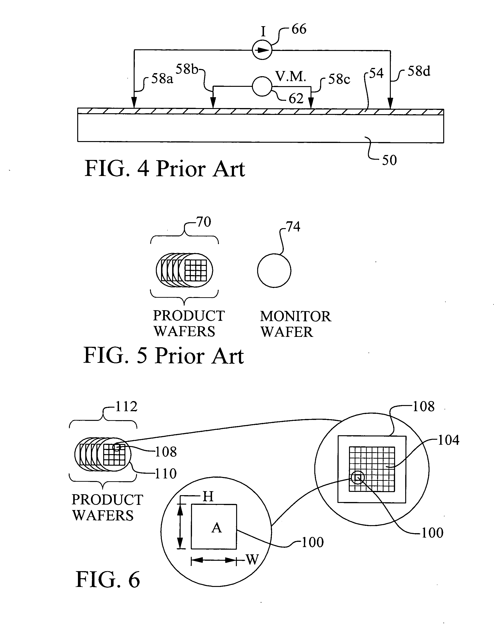
[0024]FIGS. 6 through 10 illustrate the preferred embodiment of the present invention. Several important features of the present invention are shown and discussed below. Referring particularly to FIG. 6, a new method for monitoring metal silicide sheet resistance is shown. In this method, the measurement is performed via an optical measuring system that measures the sheet resistance on the product wafers 112. Each prod...


PUM

PropertyMeasurementUnit
surface areaaaaaaaaaaa
areaaaaaaaaaaa
widthaaaaaaaaaa

Abstract

A new method to monitor sheet resistance of a metal silicide layer in the manufacture of an integrated circuit device is achieved. The method comprises providing a metal silicide layer overlying an exposed silicon layer on a substrate. A thermal wave intensity signal is generated for the metal silicide layer by an optical measurement system. The optical measurement system comprises a first laser beam that is intensity modulated and a second laser beam. The first and second laser beams comprise different wavelengths. A dichroic mirror is used to combine the first and second laser beams and to project the first and second laser beams onto the metal silicide layer. A detector is used to gather the second laser beam reflected from the metal silicide layer and to generate a thermal wave intensity signal based on the reflected second laser beam. Sheet resistance of the metal silicide layer is calculated by a linear equation based on the thermal wave intensity signal.

Description

BACKGROUND OF THE INVENTION [0001] 1. Field of the Invention [0002] The invention relates to a method of manufacturing an integrated circuit device, and, more particularly, to a method of monitoring silicide formation. [0003] 2. Description of the Prior Art [0004] Metal silicide thin films are frequently used in the art of integrated circuit manufacturing. Metal silicide provides a means to reduce the resistance of gate, source, and drain regions in MOS devices. A typical metal silicide application is shown in FIGS. 1 through 3. Referring particularly to FIG. 1, a cross section of a partially completed integrated circuit device is illustrated. MOS transistors are formed on a silicon substrate 10. Each transistor comprises a polysilicon layer 22 overlying an oxide layer 18 to form a gate and heavily doped source and drain regions 14. In addition, dielectric spacers 26 are formed on the sidewalls of the gates 22 as part of the lightly doped drain process that is well known in the art....

Claims


Application Information

Patent Timeline
Patent Type & Authority Applications(United States)
IPC IPC(8): G01N21/17G01R31/28
CPCG01R31/2831G01N21/1717
Inventor MAURY, ALVAROLAYADI, NACELIM, JOVIN
Owner CHARTERED SEMICONDUCTOR MANUFACTURING
Why Eureka
Try Eureka