Method for forming bit-line of semiconductor device
- Summary
- Abstract
- Description
- Claims
- Application Information
AI Technical Summary
Benefits of technology
Problems solved by technology
Method used
Image

Examples
Embodiment Construction
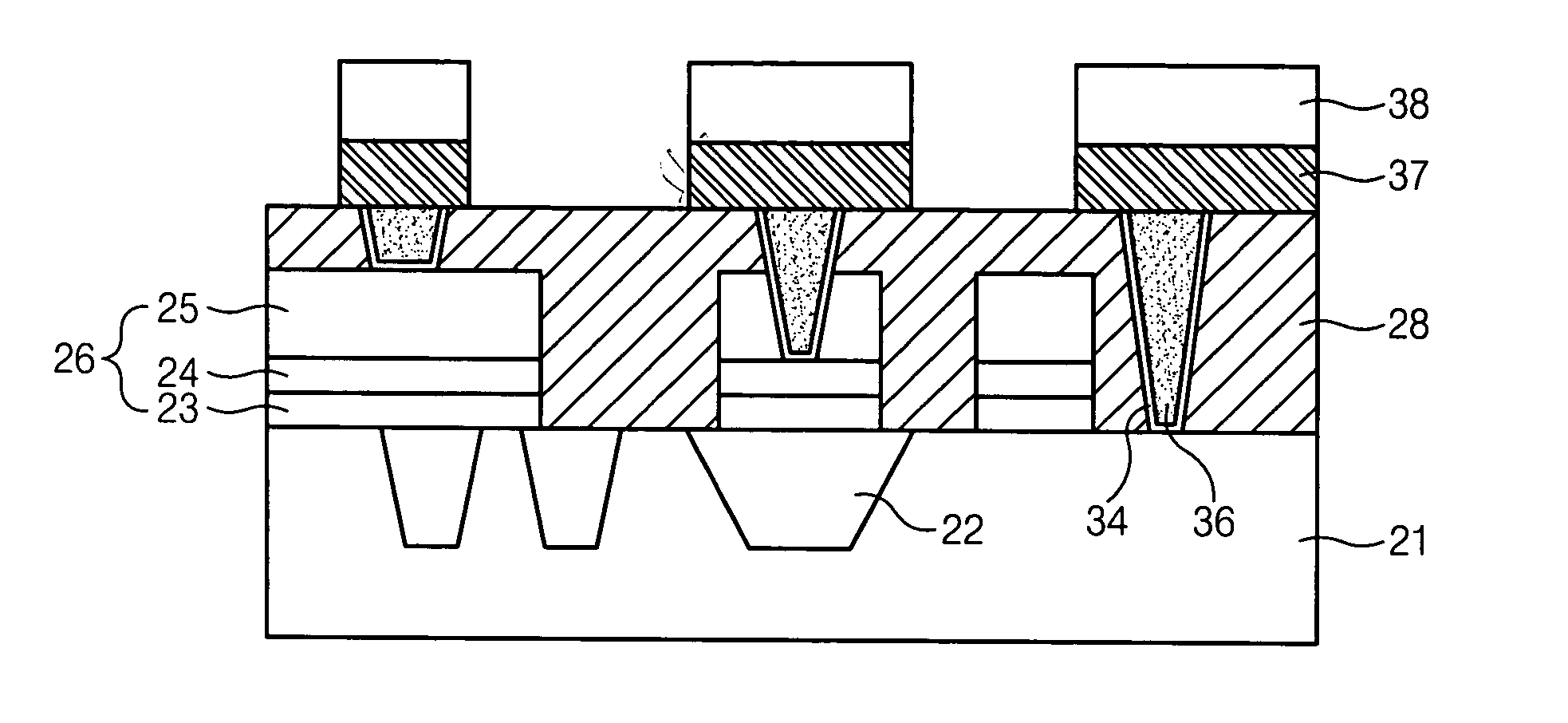
[0030] Hereinafter, the present invention will be described in detail with reference to the accompanying drawings.
[0031]FIGS. 2a to 2e are cross-sectional diagrams illustrating a method for forming a bit-line according to an embodiment of the present invention.
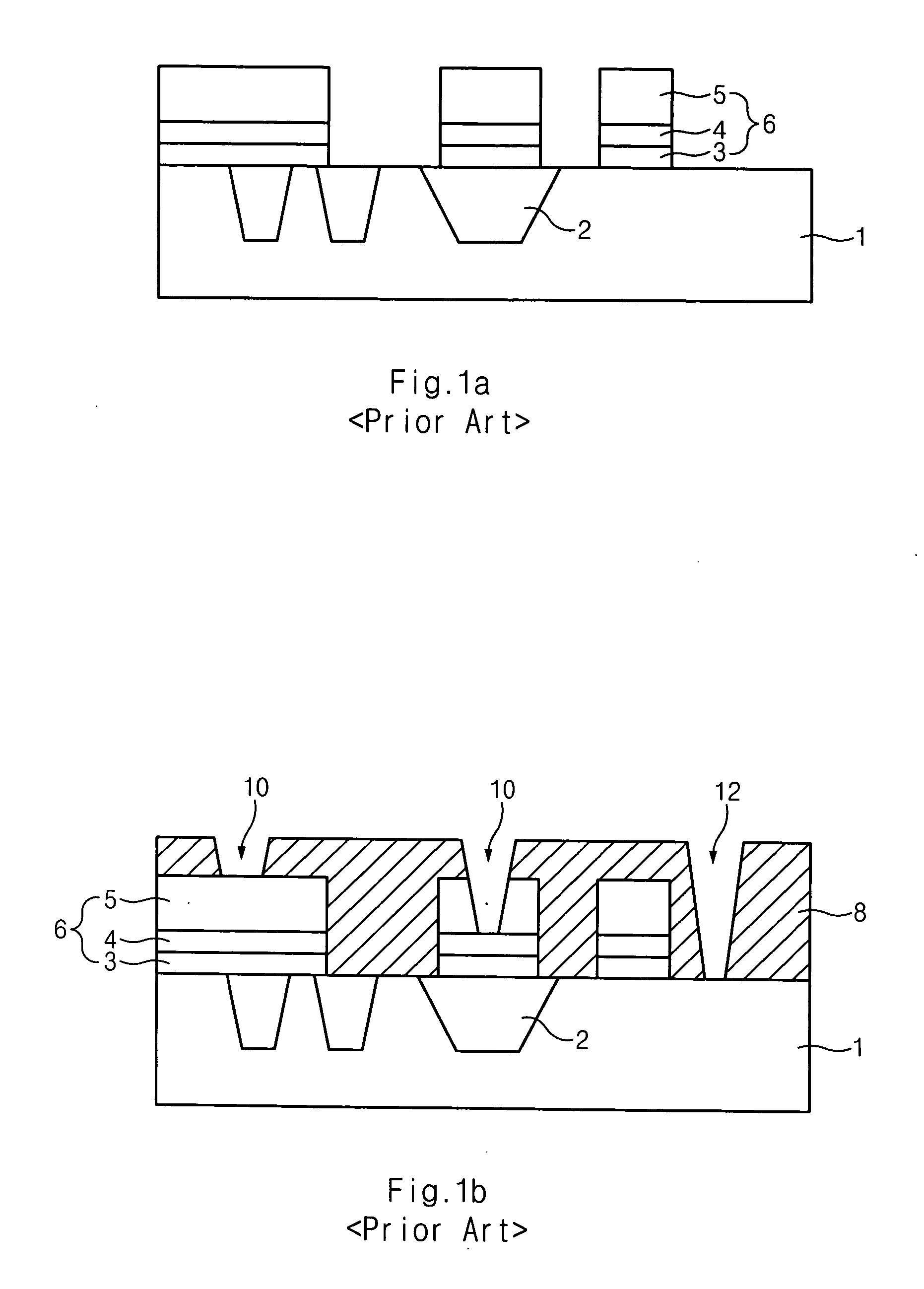
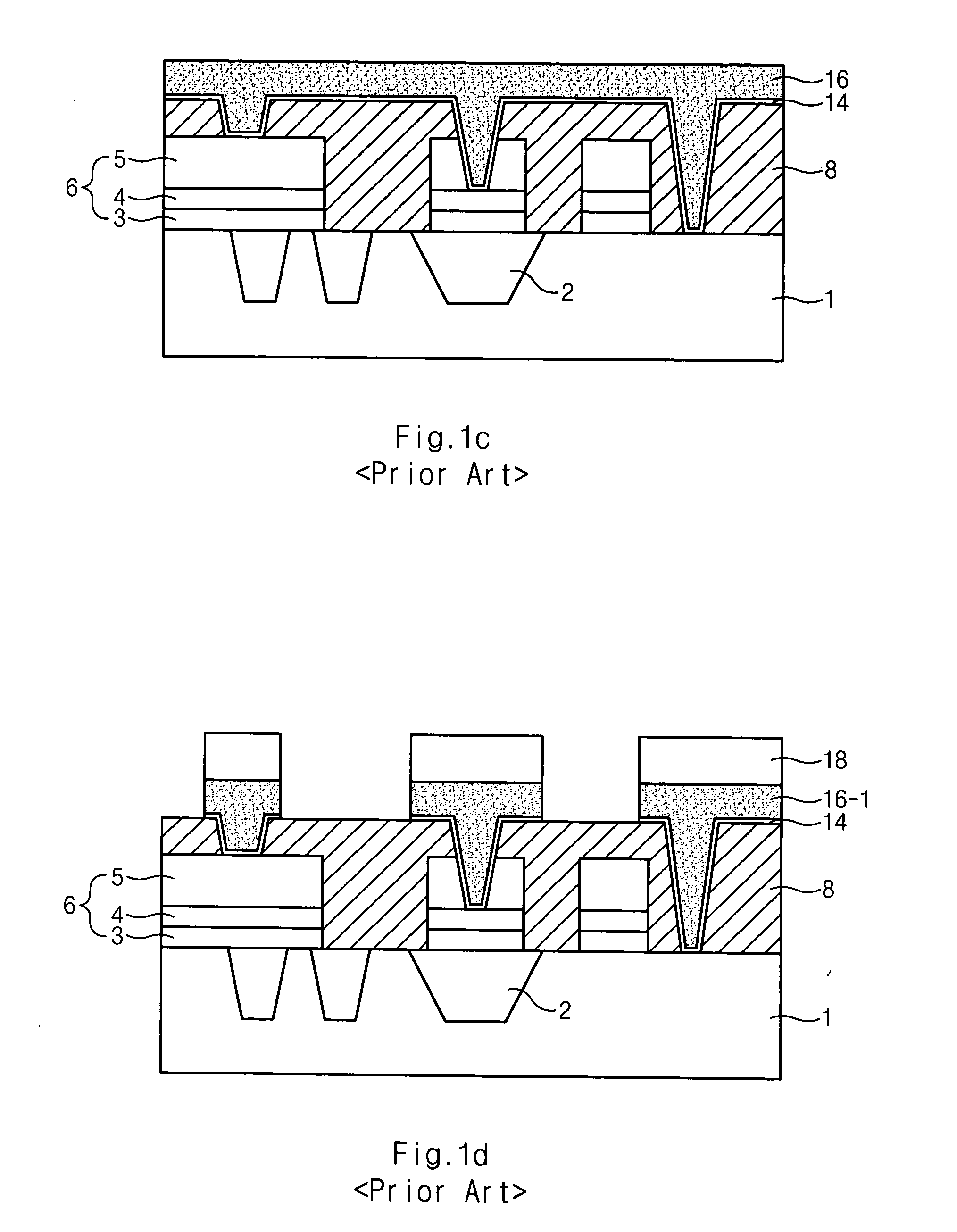
[0032] Referring to FIG. 2a, a polysilicon layer (not shown), a conductive layer for gate electrode (not shown) and a hard mask nitride film (not shown) are sequentially formed on a semiconductor substrate 21 comprising a device isolation film 22.
[0033] A selective etching process is performed on the hard mask nitride film (not shown), the conductive layer for gate electrode (not shown) and the polysilicon layer (snot shown). Then, a gate line 26 where a polysilicon pattern 23, a conductive pattern for gate electrode 24 and a hard mask nitride film pattern 25 are sequentially stacked is formed.
[0034] As shown in FIG. 2b, an interlayer insulating film (not shown) is formed on the semiconductor substrate including the gate l...
PUM
 Abstract
Description
Claims
Application Information
 - R&D
- Intellectual Property
- Life Sciences
- Materials
- Tech Scout
- Unparalleled Data Quality
- Higher Quality Content
- 60% Fewer Hallucinations
Browse by: Latest US Patents, China's latest patents, Technical Efficacy Thesaurus, Application Domain, Technology Topic, Popular Technical Reports.
© 2025 PatSnap. All rights reserved.Legal|Privacy policy|Modern Slavery Act Transparency Statement|Sitemap|About US| Contact US: help@patsnap.com