Attachment of integrated circuit structures and other substrates to substrates with vias

a technology of integrated circuits and substrates, applied in the direction of semiconductor devices, semiconductor/solid-state device details, electrical apparatus, etc., can solve the problems of mechanical and thermal weakening of solder joints, increased fatigue stresses on solder joints, etc., to improve the strength and electrical conductivity of bonds

Active Publication Date: 2005-06-23
INVENSAS CORP
View PDF19 Cites 98 Cited by
  • Summary
  • Abstract
  • Description
  • Claims
  • Application Information

AI Technical Summary

Benefits of technology

[0012] In FIG. 2, an optional conductive film 220 (e.g. metal) is formed on the bottom and sidewalls of each cavity 210. Film 220 is believ...

Problems solved by technology

As the solder bump sizes decrease to accommodate the smaller contact pads and pitches, the solder joints become mechanically and thermally weaker.
If the standoff is too small, there will be increas...

Method used


Image

  • Attachment of integrated circuit structures and other substrates to substrates with vias
  • Attachment of integrated circuit structures and other substrates to substrates with vias
  • Attachment of integrated circuit structures and other substrates to substrates with vias

Examples


Embodiment Construction

[0022] The embodiments described in this section illustrate but do not limit the invention. The invention is not limited to particular materials, process steps, or dimensions. The invention is defined by the appended claims.

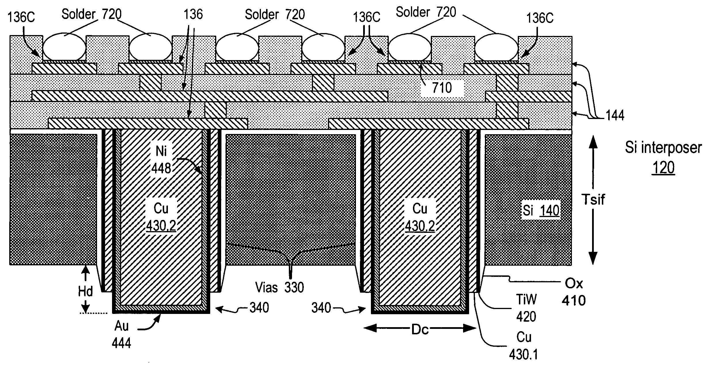
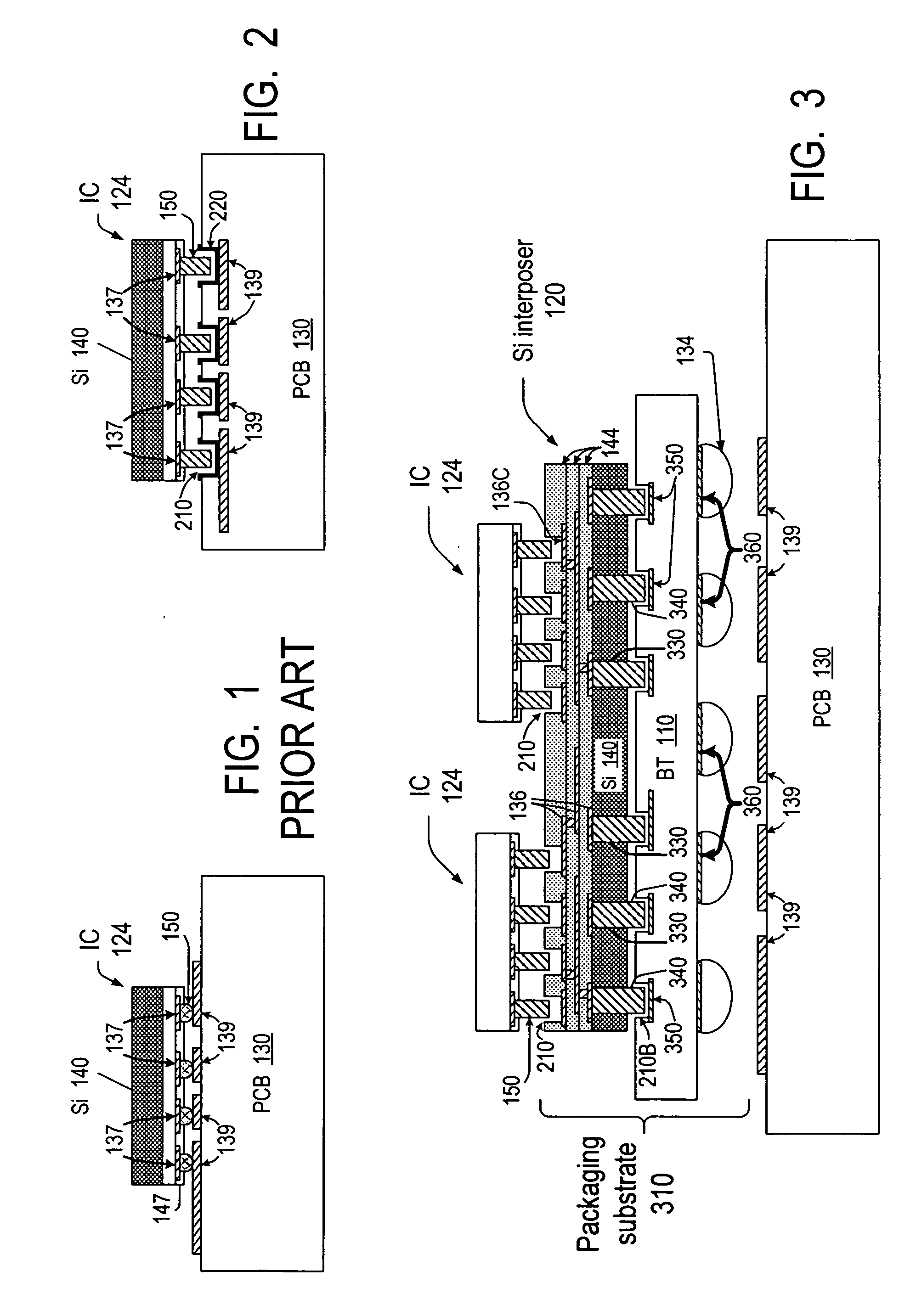
[0023]FIG. 3 illustrates another integrated circuit packaging structure. Integrated circuit packaging substrate 310 is an intermediate substrate that provides an interconnection between dies 124 and PCB 130. Substrate 310 includes two intermediate integrated circuit packaging substrates 110, 120. Substrate 120 is a silicon interposer attached to BT substrate 110, and thus is itself a semiconductor integrated circuit. The attachment is made as described above in connection with FIG. 2. More particularly, cavities 210B (also called vias or openings herein) are formed in the top surface of BT substrate 110. Protruding contact pads 340 of interposer 120 are inserted into the cavities.

[0024] Dies 124 are attached to interposer 120 as in FIG. 2. More particularly, ca...


PUM


Abstract

Vias (210, 210B) are formed in a surface of a substrate. At least portions of contact pads (139, 350) are located in the vias. Contact pads (150, 340) of an integrated circuit structure are inserted into the vias and attached to the contact pads (139, 350) of the substrate. The vias provide a strong, reliable mechanical and electrical connection. A via may expose not only a contact pad (350) in the substrate but also a surrounding region. Solder (930) wets the contact pad better than the surrounding region, resulting in a stronger solder joint and better electrical conductivity. Alternatively, the contact may include multiple conductive layers (910.1, 910.2), with the top layer (910.2) being more solder wettable than the bottom layer (910.1) and the top layer covering only a portion of the bottom layer.

Description

CROSS REFERENCE TO RELATED APPLICATIONS [0001] The present application is a continuation-in-part of U.S. patent application Ser. No. 10 / 739,788 filed on Dec. 17, 2003 by S. Savastiouk et al., entitled “INTEGRATED CIRCUITS AND PACKAGING SUBSTRATES WITH CAVITIES, AND ATTACHMENT METHODS INCLUDING INSERTION OF PROTRUDING CONTACT PADS INTO CAVITIES”, incorporated herein by reference.BACKGROUND OF THE INVENTION [0002] The present invention relates to attachment of integrated circuits to other substrates. [0003] Integrated circuit dies (“chips”) can be attached to a lead frame and then packaged in a ceramic or plastic carrier. The leads of the lead frame can then be soldered to a printed circuit board (PCB). Alternatively, the chip can be soldered directly to the PCB (“flip chip” packaging). The flip chip packaging reduces the package size and shortens the electrical connections between the die and the PCB. FIG. 1 illustrates a chip 124 flip-chip attached to a PCB 130. The chip is attached...

Claims


Application Information

Patent Timeline
IPC IPC(8): H01L23/14H01L23/48H01L23/498H01L23/538H01L25/065
CPCH01L23/13H01L23/147H01L2924/10253H01L2224/45144H01L2224/73204H01L2224/32225H01L2224/16225H01L2924/01322H01L2224/16227H01L24/48H01L2924/30107H01L2924/19041H01L2924/15311H01L2924/01079H01L2924/01078H01L2224/48227H01L23/49811H01L23/49816H01L23/49822H01L23/49827H01L23/5384H01L23/5385H01L25/0655H01L2224/13022H01L2224/16237H01L2224/48091H01L2924/00014H01L2924/00H01L2924/12042H01L24/45H01L2924/14H01L2924/19107H01L21/76898H01L23/481H01L2224/10126H01L2224/45099
Inventor SAVASTIOUK, SERGEYKAO, SAM
Owner INVENSAS CORP
Why Eureka
Try Eureka