Bio-optical sensors

a biooptical sensor and optical sensor technology, applied in the field of biooptical sensors, can solve the problems of inaccurate calibration signal, change in device conditions, time difference between the acquisition of dark reference frame, etc., and achieve the effect of increasing system sensitivity, accurate calibration signal, and less analy

Inactive Publication Date: 2005-06-30
STMICROELECTRONICS (RES & DEV) LTD
View PDF11 Cites 12 Cited by
  • Summary
  • Abstract
  • Description
  • Claims
  • Application Information

AI Technical Summary

Benefits of technology

[0007] An object of the present invention is to provide a bio-optical sensor having a more accurate calibration signal. A more accura...

Problems solved by technology

This means that there is a time difference between the acquisition of the dark reference frame and the detection and processing of the sensor signal.
During this time there may be changes in the conditions on the device, e.g., operating vo...

Method used


Image

  • Bio-optical sensors
  • Bio-optical sensors
  • Bio-optical sensors

Examples


Embodiment Construction

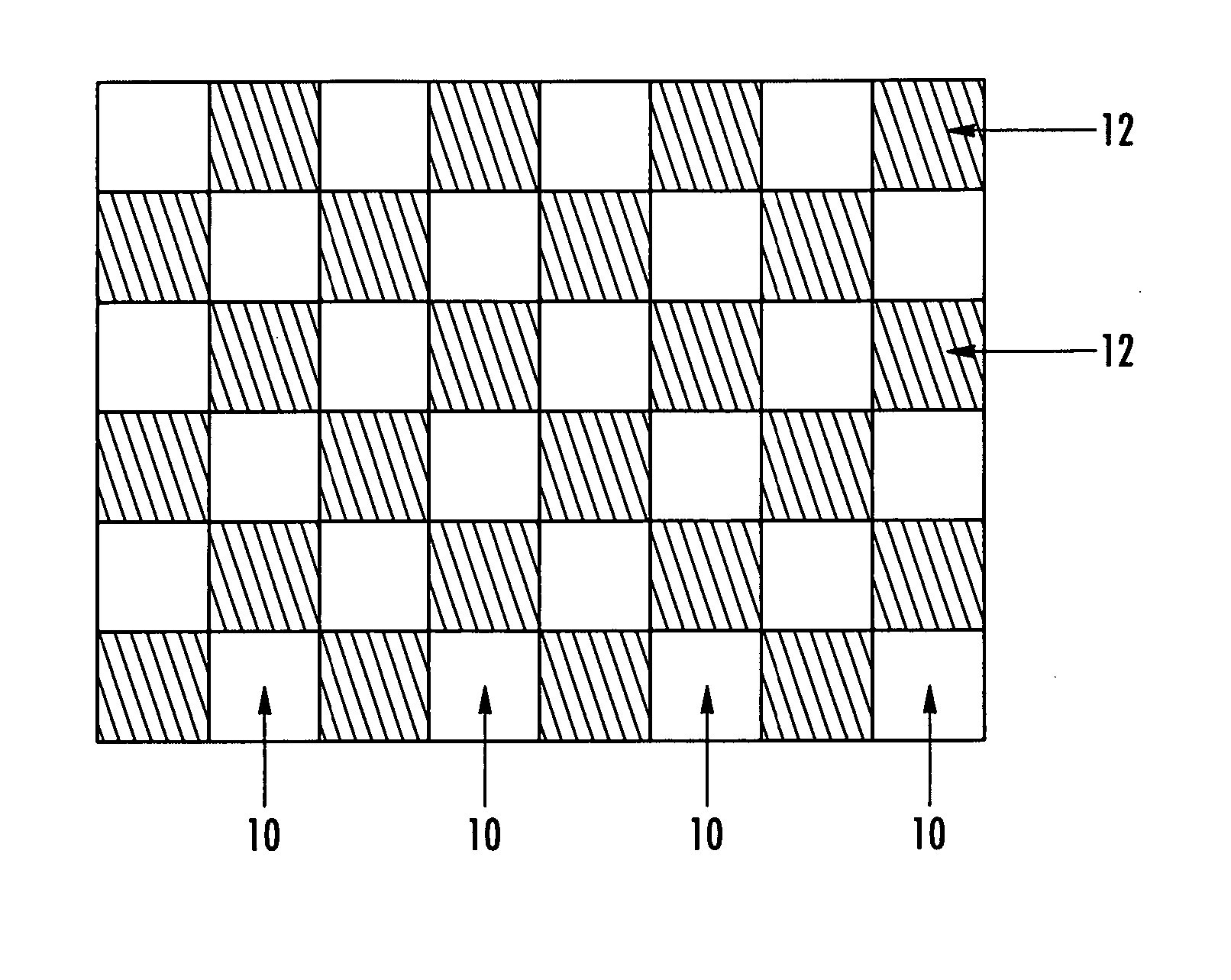
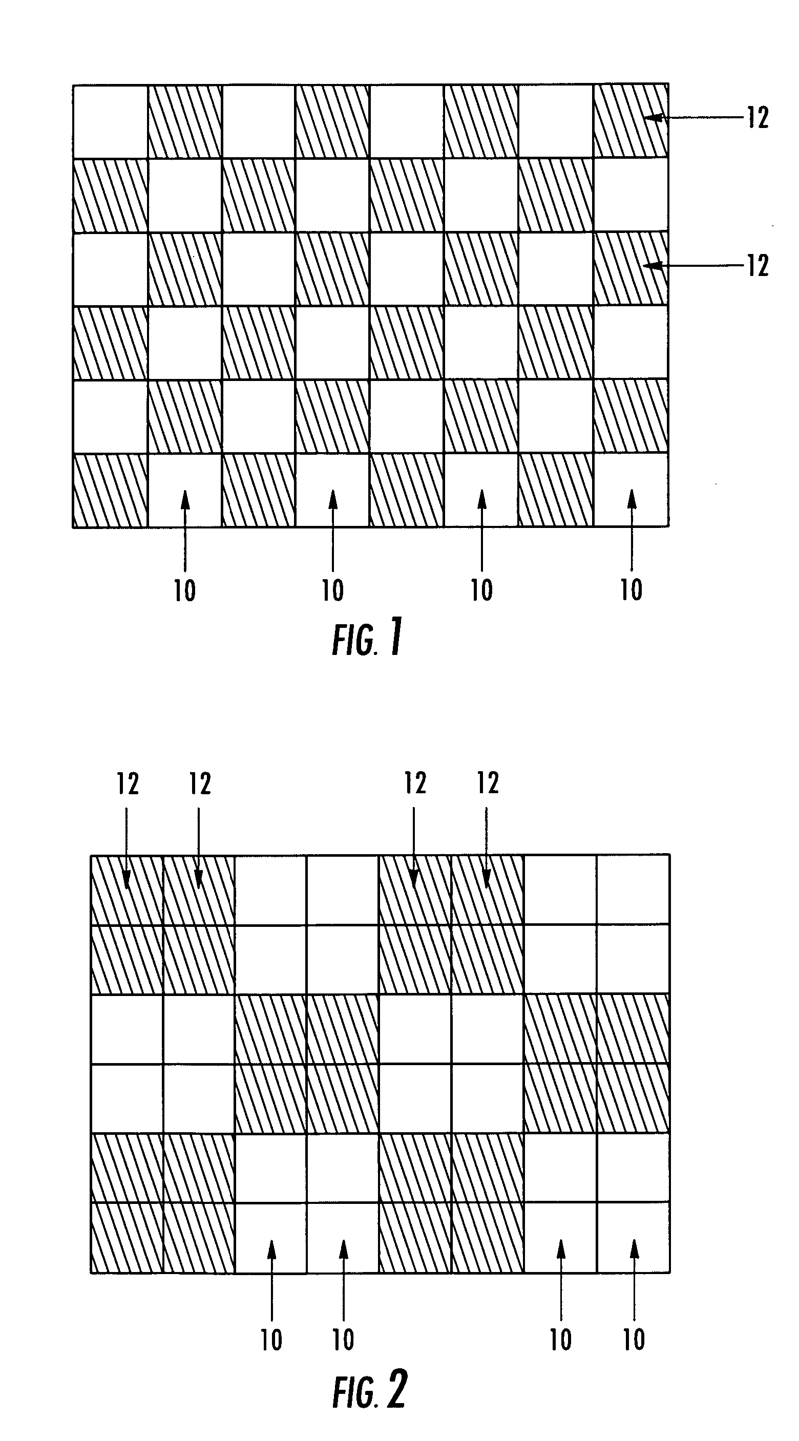
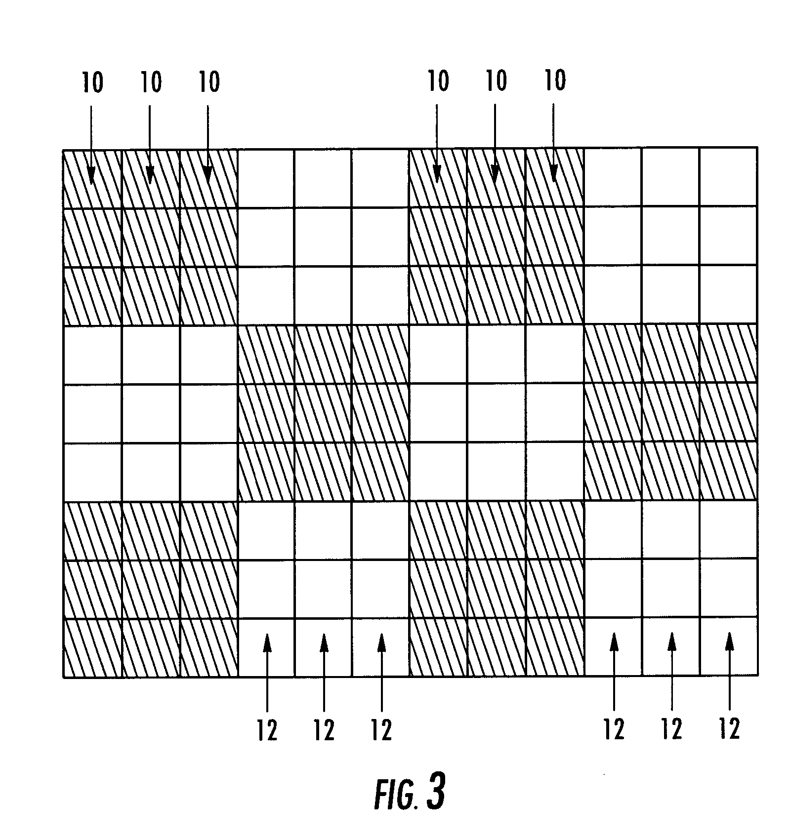
[0015]FIG. 1 shows a straightforward form of the invention in which the image surface is divided into sensing pixels 10 and calibration pixels 12 which are interleaved on a 1:1 basis, i.e., in a checker board fashion. Each of the pixels 10, 12 is an imaging pixel of a well-known type, such as a 3-transistor or 4-transistor pixel based on CMOS technology. The calibration pixels 12 are shielded from light by a suitable mask, which may be printed on top of the array or may be formed by selective metallization during fabrication, for example. When a metal mask is used, there is preferably a layer separated from the readout electronics to reduce parasitic capacitance.

[0016] Alternatives to metallization for forming the opaque layer include silicided gate oxide, and superposition of color filters, i.e., overlaying red green and blue filters to give black.

[0017] It is preferable that the border pixels situated at the edge of the sensor are not used, either for sensing or calibration. The...


PUM


Abstract

A bio-optical sensor has a surface provided with an array of sensing pixels and calibration pixels. The sensing and calibration pixels are arranged in an interleaved fashion. The sensing and calibration pixels may be interleaved 1:1, or they may be arranged in interleaved blocks. The image plane receives an analyte and a reagent that reacts with the analyte to produce light. The sensing pixels generate signals as a function of the light produced.

Description

FIELD OF THE INVENTION [0001] The present invention relates to bi-optical sensors, and in particular, to a light-sensitive semiconductor device for detecting and measuring light emitted by the reaction of a reagent with a biological sample. BACKGROUND OF THE INVENTION [0002] In known bio-optical sensors, the reaction takes place on a surface of the semiconductor device which is an image surface divided into pixels. The light produced by reactions of this nature is small, and accordingly, the signal produced by any pixel of the device is also small. The signal is frequently less than other effects such as dark current (leakage current) from the pixel and voltage offsets. Therefore, a calibration / cancellation scheme may be necessary to increase the sensitivity of the system. [0003] In the related field of solid state image sensors, there are a number of known calibration techniques. In image sensors, it may be necessary to have a continuous image plane on which the image is formed. Ca...

Claims


Application Information

Patent Timeline
IPC IPC(8): G01N21/25G01N21/27G01N21/64G01N21/75
CPCG01N21/253G01N21/274G01N21/75G01N21/6454G01N21/6428
Inventor RAYNOR, JEFFREY
Owner STMICROELECTRONICS (RES & DEV) LTD
Why Eureka
Try Eureka