Light emitting device and fabrication method thereof

a technology of light emitting device and fabrication method, which is applied in the direction of lasers, semiconductor lasers, lighting and heating apparatus, etc., can solve the problems of low light extraction efficiency, fraction of consumed electrical input contributing to externally observable light, and achieve the effect of improving light extraction efficiency

Inactive Publication Date: 2005-06-30
SANYO ELECTRIC CO LTD
View PDF15 Cites 68 Cited by
  • Summary
  • Abstract
  • Description
  • Claims
  • Application Information

AI Technical Summary

Benefits of technology

[0019] It is an object of the present invention to provide a light emitting device having a sufficiently improved light extraction efficiency without causing defects in the light emitting device structure and the fabrication method thereof.

Problems solved by technology

A problem with LEDs is a low light extraction efficiency.
The low light extraction efficiency is caused by only a fraction of the light energy produced by a light emitting layer (i.e., active layer) emitted out of an LED as light.
As a consequence of the low light extraction efficiency, only a fraction of consumed electrical input contributes to externally observable light.
The method described in JP 2003-17740 A offers a higher light extraction efficiency by processing a semiconductor itself; but on the other hand, easily introduces defects in the substrate due to the damage caused by heating the semiconductor at high temperature for stamping.

Method used


Image

  • Light emitting device and fabrication method thereof
  • Light emitting device and fabrication method thereof
  • Light emitting device and fabrication method thereof

Examples


examples

[0139] The present invention will, hereinafter, be described in more detail through Examples, by which the invention shall not be limited.

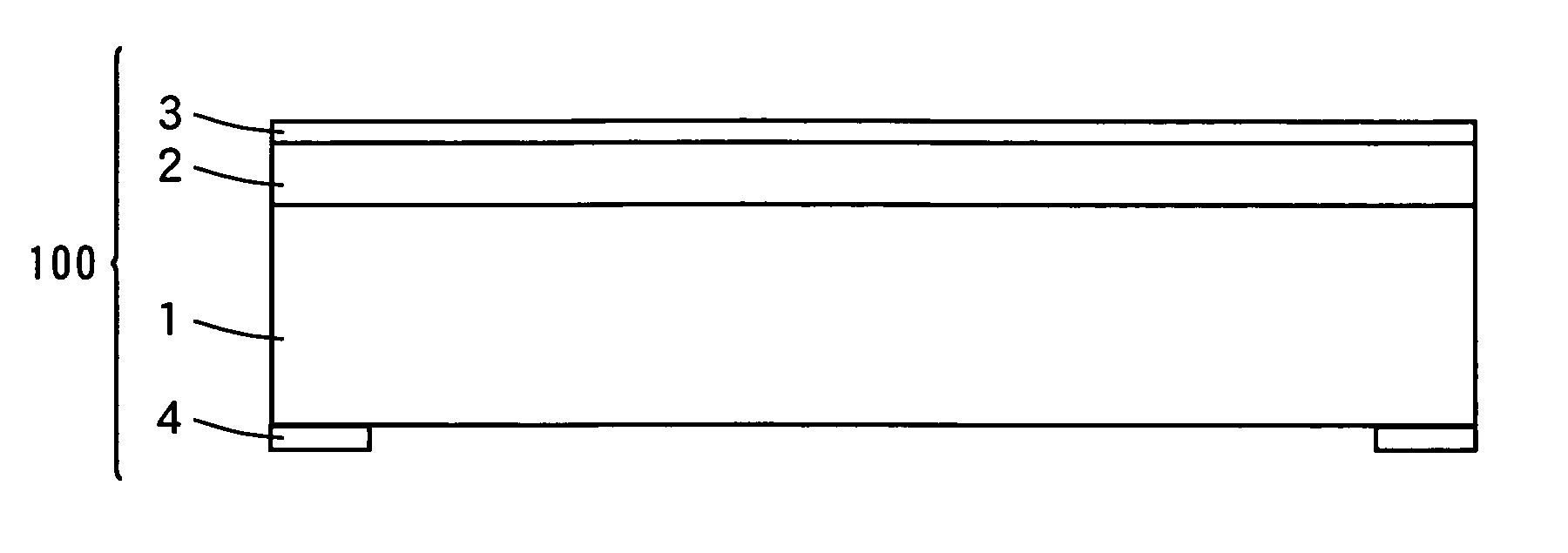
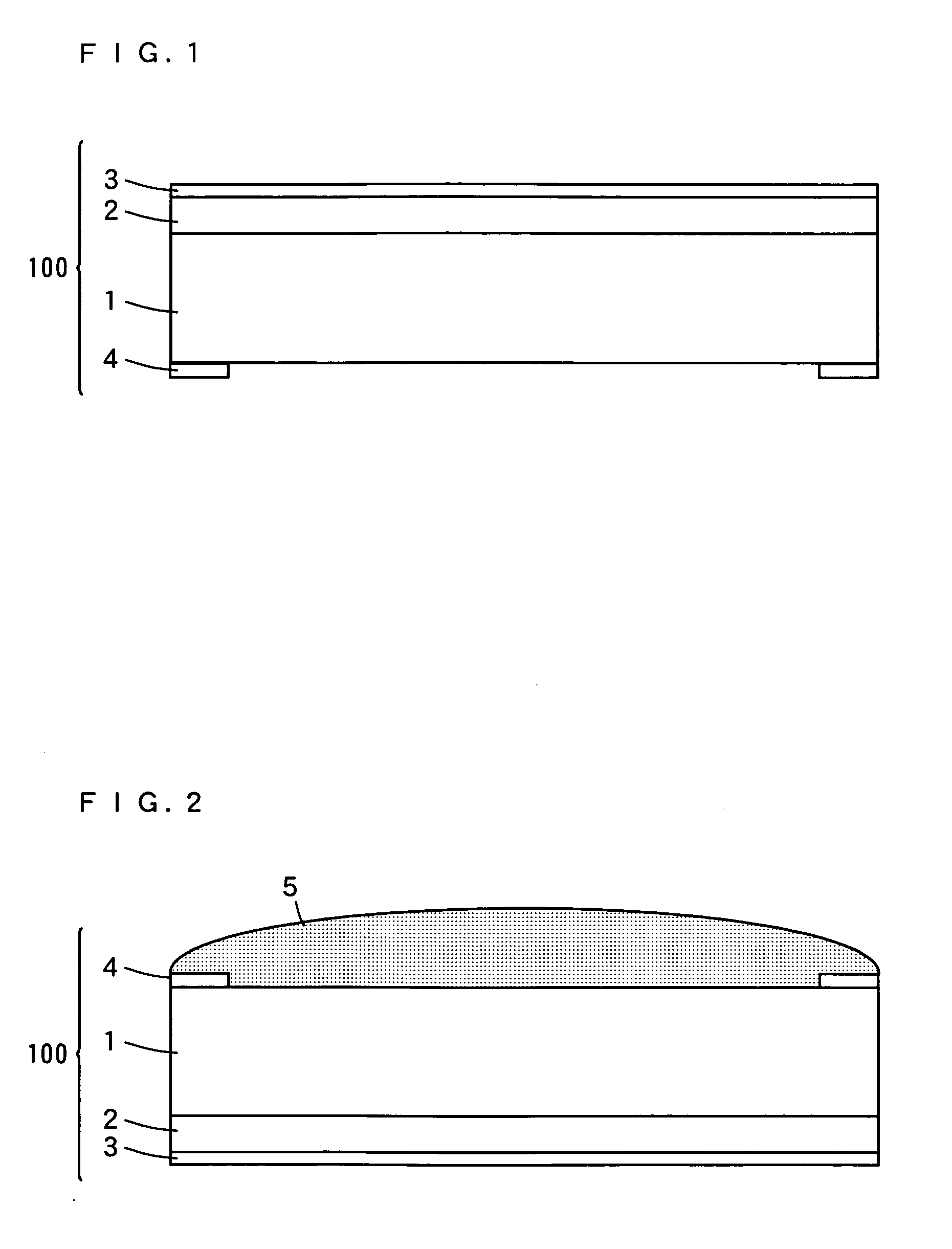
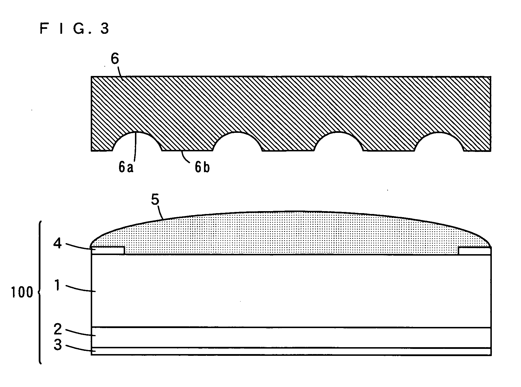
[0140] In Inventive Examples 1 to 5 and 7 to 10, light emitting devices having the structure shown in FIGS. 1 to 5 were fabricated, whereas in Inventive Example 6, a light emitting device having the structure shown in FIG. 6 was fabricated. The light emitting device structures 100 of the light emitting devices in the Inventive Examples 1, 2, 4 to 10 are the GaN-based LEDs as shown in FIG. 7. The light emitting device structure 100 of the light emitting device in the Inventive Example 3 is the ZnO-based LED as shown in FIG. 8.

[0141] In Comparative Example, a light emitting device having the light emitting device structure 100 as shown in FIG. 7, without an inorganic material layer, was fabricated.

[0142] The light emitting devices measure 1 mm per side. In each of the light emitting devices, an n-electrode 4 was formed on the outer peripheral reg...


PUM

PropertyMeasurementUnit
transparentaaaaaaaaaa
refractive indexaaaaaaaaaa

Abstract

A pre-curing viscous solution (precursor solution) is applied to the back surface of a substrate for forming an optically transparent layer principally composed of an inorganic material. The substrate is heated or irradiated with UV light while being pressed with unevenness of a mold. By removing the substrate from the mold, the optically transparent, inorganic material layer principally composed of the inorganic material is formed on the substrate. In this manner, the inorganic material layer with the unevenness is formed on the back surface of the substrate (a light extraction surface) by embossing.

Description

BACKGROUND OF THE INVENTION [0001] 1. Field of the Invention [0002] The present invention relates to a light emitting device having a light emitting device structure and the fabrication method thereof. [0003] 2. Description of the Background Art [0004] Light emitting diodes (LEDs) are capable of emitting electromagnetic waves in ultraviolet (UV), visible, or infrared (IR) regions of the electromagnetic spectrum. The LEDs emitting UV light and visible light are used for illumination and displays. [0005] A problem with LEDs is a low light extraction efficiency. Light extraction efficiency is defined as the ratio of the number of photons emitted out of the LED to the number of photons produced in the LED. The low light extraction efficiency is caused by only a fraction of the light energy produced by a light emitting layer (i.e., active layer) emitted out of an LED as light. In the case of an AlGaAs-based LED with a transparent substrate, for example, about 30% of the light energy prod...

Claims


Application Information

Patent Timeline
Patent Type & Authority Applications(United States)
IPC IPC(8): F21V7/00H01L33/22H01L33/32H01L33/48H01S5/00
CPCH01L33/44H01L33/54H01L33/58H01L2924/0002H01L2924/00
Inventor HATA, MASAYUKIHIROYAMA, RYOJIKUNISATO, TATSUYAKURAMOTO, KEIICHIHIRANO, HITOSHI
Owner SANYO ELECTRIC CO LTD
Why Eureka
Try Eureka